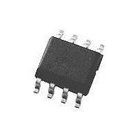
LM3477MM National Semiconductor, LM3477MM Datasheet - Page 17

LM3477MM
Manufacturer Part Number
LM3477MM
Description
Pulse Width Modulation (PWM) Controller IC
Manufacturer
National Semiconductor
Specifications of LM3477MM
Input Voltage Primary Min
2.95V
Mounting Type
Surface Mount
Topology
Buck (Step Down)
Control Mode
Current
Duty Cycle Max
93%
Input Voltage Primary Max
35V
Lead Free Status / RoHS Status
Contains lead / RoHS non-compliant
Available stocks
Company
Part Number
Manufacturer
Quantity
Price
Part Number:
LM3477MM
Manufacturer:
NS/国半
Quantity:
20 000
Part Number:
LM3477MM/NOPB
Manufacturer:
NS/国半
Quantity:
20 000
Part Number:
LM3477MMX
Manufacturer:
NS/国半
Quantity:
20 000
Company:
Part Number:
LM3477MMX/NOPB
Manufacturer:
TI
Quantity:
6 223
Output Capacitor Selection
How the output voltage recovers after that initial excursion
depends on how fast the inductor current falls and how large
the output capacitance is. See Figure 10.
The ESR and the capacitance of the output capacitor must
be carefully chosen so that the output voltage overshoot is
within the design’s specification V
bined ESR of the output capacitors is not low enough, the
initial output voltage excursion will violate the specification,
see ∆V
output capacitance, the output voltage will travel outside the
specification window due to the extra charge being dumped
into the capacitor, see ∆V
voltage protection (OVP) which could trigger if the transient
overshoot is high enough. If this happens, the controller will
operate in hysteretic mode (see OVER VOLTAGE PROTEC-
TION section) for a few cycles before the output voltage
settles to its steady state. If this behavior is not desired,
substitute V
found in the ELECTRICAL CHARACTERISTICS table) to
find the minimum capacitance and maximum ESR of the
output capacitor.
Calculations for the Output Capacitor
During a loading transient, the delta output voltage ∆V
two changing components. One is the voltage difference
across the ESR (∆V
caused by the gained charge (∆V
The design objective is to keep ∆V
mum overshoot (V
the output load requirements.
Both voltages ∆V
equation is:
where,
R
∆I
I
D
Evaluating this equation at t = 0 gives ∆V
V
OUT(MAX)
(Continued)
OS(MAX)
ESR
MIN
OUT
FIGURE 10. Output Voltage Overshoot Violation
= Minimum duty cycle of device (0.165 typical)
= the output capacitor ESR
= the difference between the load current change
C1
. If the ESR is low enough, but there is not enough
for ∆V
− I
OVP
OUT(MIN)
(referred to the output) for V
r(MAX)
r
and ∆V
OS(MAX)
r
∆V
), the other is the voltage difference
and solving for R
c
C2
q
= ∆V
). V
will change with time. For ∆V
. The LM3477/A has output over
OS(MAX)
r
+ ∆V
q
OS(MAX)
). This gives:
c
lower than some maxi-
q
is chosen based on
ESR
r(max)
. If the total com-
OS(MAX)
gives:
. Substituting
200033B5
(V
OVP
c
r
has
the
is
17
The expression for ∆V
From Figure 11 it can be told that ∆V
value at some point in time and then decrease. The larger
the output capacitance is, the earlier the peak will occur. To
find the peak position, let the derivative of ∆V
and the result is:
The intention is to find the capacitance value that will yield, at
t
equating ∆V
C
The chosen output capacitance should not be less than
47µF, even if the solution for C
Notice it is already assumed that the total ESR is no greater
than R
will be a negative number.
Power MOSFET Selection
The drive pin of LM3477/A must be connected to the gate of
an external MOSFET. In a buck topology, the drain of the
external N-Channel MOSFET is connected to the input and
the source is connected to the inductor. The C
provides the gate drive needed for an external N-Channel
MOSFET. The gate drive voltage depends on the input volt-
age (see TYPICAL PERFORMANCE CHARACTERISTICS).
In most applications, a logic level MOSFET can be used. For
very low input voltages, a sub-logic level MOSFET should be
used.
The selected MOSFET directly controls the efficiency. The
critical parameters for selection of a MOSFET are:
1. Minimum threshold voltage, V
2. On-resistance, R
peak
OUT(MIN)
, a ∆V
FIGURE 11. Output Voltage Overshoot Peak
ESR(MAX)
:
C
that equals V
C
to V
, otherwise the term under the square root
OS(max)
DS
q
(ON)
is:
OS(max)
gives the following solution for
. Substituting tpeak for t and
OUT(MIN)
TH
(MIN)
C
will reach its peak
is less than 47µF.
C
B
www.national.com
go to zero,
pin voltage
200033B6


