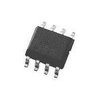
LM2663M National Semiconductor, LM2663M Datasheet - Page 6

LM2663M
Manufacturer Part Number
LM2663M
Description
DC/DC Charge Pump Converter IC
Manufacturer
National Semiconductor
Specifications of LM2663M
Output Current
200mA
No. Of Pins
8
Power Dissipation Pd
735mW
Mounting Type
Surface Mount
Peak Reflow Compatible (260 C)
No
Supply Voltage Max
5.5V
Leaded Process Compatible
No
Lead Free Status / RoHS Status
Contains lead / RoHS non-compliant
Available stocks
Company
Part Number
Manufacturer
Quantity
Price
Part Number:
LM2663M
Manufacturer:
NS/国半
Quantity:
20 000
Company:
Part Number:
LM2663M/NOPB
Manufacturer:
TI
Quantity:
9 140
Part Number:
LM2663MX
Manufacturer:
NS/国半
Quantity:
20 000
Company:
Part Number:
LM2663MX/NOBP
Manufacturer:
AMIS
Quantity:
6 224
Company:
Part Number:
LM2663MX/NOPB
Manufacturer:
ZARLINK
Quantity:
450
Part Number:
LM2663MX/NOPB
Manufacturer:
TI/德州仪器
Quantity:
20 000
www.national.com
Connection Diagrams
8-Lead SO (M)
Pin Description
Circuit Description
The LM2662/LM2663 contains four large CMOS switches
which are switched in a sequence to invert the input supply
voltage. Energy transfer and storage are provided by exter-
nal capacitors. Figure 2 illustrates the voltage conversion
scheme. When S
supply voltage V+. During this time interval switches S
S
and S
of cycles, the voltage across C
the anode of C
cathode of C
in the switches, and no ESR in the capacitors. In reality, the
charge transfer efficiency depends on the switching fre-
quency, the on-resistance of the switches, and the ESR of
the capacitors.
Pin
4
1
1
2
3
4
5
6
7
8
are open. In the second time interval, S
2
and S
(LM2662)
(LM2663)
Name
CAP+
CAP−
GND
OUT
OSC
2
4
SD
FC
V+
LV
equals −(V+) assuming no load on C
are closed, C
2
is connected to ground, the output at the
1
and S
Frequency control for internal oscillator:
FC = open, f
FC = V+, f
FC has no effect when OSC pin is driven
externally.
Shutdown control pin, tie this pin to the ground in
normal operation.
Connect this pin to the positive terminal of
charge-pump capacitor.
Power supply ground input.
Connect this pin to the negative terminal of
charge-pump capacitor.
Negative voltage output.
Low-voltage operation input. Tie LV to GND
when input voltage is less than 3.5V. Above
3.5V, LV can be connected to GND or left open.
When driving OSC with an external clock, LV
must be connected to GND.
Oscillator control input. OSC is connected to an
internal 15 pF capacitor. An external capacitor
can be connected to slow the oscillator. Also, an
external clock can be used to drive OSC.
Power supply positive voltage input.
3
1
are closed, C
is charging C
2
will be pumped to V+. Since
10000320
OSC
OSC
= 150 kHz (typ);
Voltage Inverter
= 20 kHz (typ);
1
1
2
and S
. After a number
charges to the
Order Number LM2662M, LM2663M
See NS Package Number M08A
3
2
are open
, no loss
2
and
Top View
6
Function
FIGURE 2. Voltage Inverting Principle
Same as inverter.
Same as inverter.
Same as inverter.
Power supply positive voltage input.
Same as inverter.
Power supply ground input.
LV must be tied to OUT.
Same as inverter except that OSC cannot be
driven by an external clock.
Positive voltage output.
Voltage Doubler
10000321
10000322


