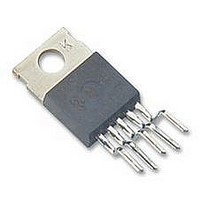
LM2576HVT-5.0 National Semiconductor, LM2576HVT-5.0 Datasheet - Page 17

LM2576HVT-5.0
Manufacturer Part Number
LM2576HVT-5.0
Description
DC/DC Converter IC
Manufacturer
National Semiconductor
Datasheets
1.LM2576SX-5.0.pdf
(24 pages)
2.LM2576SX-5.0.pdf
(24 pages)
3.LM2576SX-5.0.pdf
(22 pages)
Specifications of LM2576HVT-5.0
Input Voltage
60V
Output Voltage
5V
No. Of Pins
5
Termination Type
Through Hole
Mounting Type
Through Hole
Output Current Max
3A
Peak Reflow Compatible (260 C)
No
Supply Voltage Max
60V
Lead Free Status / RoHS Status
Contains lead / RoHS non-compliant
Available stocks
Company
Part Number
Manufacturer
Quantity
Price
Part Number:
LM2576HVT-5.0
Manufacturer:
NS/国半
Quantity:
20 000
Company:
Part Number:
LM2576HVT-5.0/NOPB
Manufacturer:
TI
Quantity:
3 000
Additional Applications
negative output voltage, then by grounding the feedback pin,
the regulator senses the inverted output voltage and regu-
lates it to −12V.
For an input voltage of 12V or more, the maximum available
output current in this configuration is approximately 700 mA.
At lighter loads, the minimum input voltage required drops to
approximately 4.7V.
The switch currents in this buck-boost configuration are
higher than in the standard buck-mode design, thus lowering
the available output current. Also, the start-up input current
of the buck-boost converter is higher than the standard
buck-mode regulator, and this may overload an input power
source with a current limit less than 5A. Using a delayed
turn-on or an undervoltage lockout circuit (described in the
next section) would allow the input voltage to rise to a high
enough level before the switcher would be allowed to turn
on.
Because of the structural differences between the buck and
the buck-boost regulator topologies, the buck regulator de-
sign procedure section can not be used to to select the in-
ductor or the output capacitor. The recommended range of
inductor values for the buck-boost design is between 68 µH
and 220 µH, and the output capacitor values must be larger
than what is normally required for buck designs. Low input
voltages or high output currents require a large value output
capacitor (in the thousands of micro Farads).
The peak inductor current, which is the same as the peak
switch current, can be calculated from the following formula:
Where f
rent operating conditions, the minimum V
worst case. Select an inductor that is rated for the peak cur-
rent anticipated.
Also, the maximum voltage appearing across the regulator is
the absolute sum of the input and output voltage. For a −12V
output, the maximum input voltage for the LM2576 is +28V,
or +48V for the LM2576HV.
The Switchers Made Simple (version 3.0) design software
can be used to determine the feasibility of regulator designs
using different topologies, different input-output parameters,
different components, etc.
NEGATIVE BOOST REGULATOR
Another variation on the buck-boost topology is the negative
boost configuration. The circuit in Figure 11 accepts an input
voltage ranging from −5V to −12V and provides a regulated
−12V output. Input voltages greater than −12V will cause the
output to rise above −12V, but will not damage the regulator.
FIGURE 10. Inverting Buck-Boost Develops −12V
osc
= 52 kHz. Under normal continuous inductor cur-
(Continued)
IN
represents the
DS011476-14
17
Typical Load Current
400 mA for V
750 mA for V
Note: Heat sink may be required.
Because of the boosting function of this type of regulator, the
switch current is relatively high, especially at low input volt-
ages. Output load current limitations are a result of the maxi-
mum current rating of the switch. Also, boost regulators can
not provide current limiting load protection in the event of a
shorted load, so some other means (such as a fuse) may be
necessary.
UNDERVOLTAGE LOCKOUT
In some applications it is desirable to keep the regulator off
until the input voltage reaches a certain threshold. An under-
voltage lockout circuit which accomplishes this task is shown
in Figure 12 , while Figure 13 shows the same circuit applied
to a buck-boost configuration. These circuits keep the regu-
lator off until the input voltage reaches a predetermined
level.
V
Note: Complete circuit not shown.
TH
FIGURE 12. Undervoltage Lockout for Buck Circuit
V
Z1
IN
IN
+ 2V
= −5.2V
= −7V
FIGURE 11. Negative Boost
BE
(Q1)
DS011476-16
www.national.com
DS011476-15


