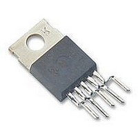
LM2575HVT-5.0 National Semiconductor, LM2575HVT-5.0 Datasheet - Page 7

LM2575HVT-5.0
Manufacturer Part Number
LM2575HVT-5.0
Description
DC/DC Converter IC
Manufacturer
National Semiconductor
Specifications of LM2575HVT-5.0
Input Voltage
60V
Output Voltage
5V
No. Of Pins
5
Termination Type
Through Hole
Mounting Type
Through Hole
Output Current Max
1A
Peak Reflow Compatible (260 C)
No
Supply Voltage Max
60V
Lead Free Status / RoHS Status
Contains lead / RoHS non-compliant
Available stocks
Company
Part Number
Manufacturer
Quantity
Price
Company:
Part Number:
LM2575HVT-5.0
Manufacturer:
NS
Quantity:
500
Part Number:
LM2575HVT-5.0
Manufacturer:
NS/国半
Quantity:
20 000
ON /OFF CONTROL Test Circuit Figure 2
V
V
I
I
Symbol
IH
IL
Specifications with standard type face are for T
Range. Unless otherwise specified, V
= 30V for the 15V version. I
IH
IL
All Output Voltage Versions
Electrical Characteristics
Note 1: Absolute Maximum Ratings indicate limits beyond which damage to the device may occur. Operating Ratings indicate conditions for which the device is in-
tended to be functional, but do not guarantee specific performance limits. For guaranteed specifications and test conditions, see the Electrical Characteristics.
Note 2: All limits guaranteed at room temperature (standard type face) and at temperature extremes (bold type face). All limts are used to calculate Average Out-
going Quality Level, and all are 100% production tested.
Note 3: All limits guaranteed at room temperature (standard type face) and at temperature extremes (bold type face). All room temperature limits are 100% pro-
duction tested. All limits at temperature extremes are guaranteed via correlation using standard Statistical Quality Control (SQC) methods.
Note 4: External components such as the catch diode, inductor, input and output capacitors can affect switching regulator system performance. When the LM1575/
LM2575 is used as shown in the Figure 2 test circuit, system performance will be as shown in system parameters section of Electrical Characteristics.
Note 5: Output (pin 2) sourcing current. No diode, inductor or capacitor connected to output pin.
Note 6: Feedback (pin 4) removed from output and connected to 0V.
Note 7: Feedback (pin 4) removed from output and connected to +12V for the Adjustable, 3.3V, and 5V versions, and +25V for the 12V and 15V versions, to force
the output transistor OFF.
Note 8: V
Note 9: Junction to ambient thermal resistance (no external heat sink) for the 5 lead TO-220 package mounted vertically, with
board with minimum copper area.
Note 10: Junction to ambient thermal resistance (no external heat sink) for the 5 lead TO-220 package mounted vertically, with
containing approximately 4 square inches of copper area surrounding the leads.
Note 11: Junction to ambient thermal resistance with approxmiately 1 square inch of pc board copper surrounding the leads. Additional copper area will lower thermal
resistance further. See thermal model in Switchers made Simple software.
Note 12: If the TO-263 package is used, the thermal resistance can be reduced by increasing the PC board copper area thermally connected to the package: Using
0.5 square inches of copper area,
Note 13: The oscillator frequency reduces to approximately 18 kHz in the event of an output short or an overload which causes the regulated output voltage to drop
approximately 40% from the nominal output voltage. This self protection feature lowers the average power dissipation of the IC by lowering the minimum duty cycle
from 5% down to approximately 2%.
Note 14: Refer to RETS LM1575J for current revision of military RETS/SMD.
Typical Performance Characteristics
Normalized Output Voltage
IN
ON /OFF Pin Logic
Input Level
ON /OFF Pin Input
Current
= 40V (60V for the high voltage version).
Parameter
JA
LOAD
DS011475-32
is 50˚C/W; with 1 square inch of copper area,
= 200 mA.
V
V
ON /OFF Pin = 5V (OFF)
ON /OFF Pin = 0V (ON)
OUT
OUT
IN
= 12V for the 3.3V, 5V, and Adjustable version, V
= 0V
= Nominal Output Voltage
(Continued)
Line Regulation
J
= 25˚C, and those with boldface type apply over full Operating Temperature
Conditions
(Circuit of Figure 2 )
7
JA
is 37˚C/W; and with 1.6 or more square inches of copper area,
DS011475-33
Typ
1.4
1.2
12
0
LM1575-XX
Dropout Voltage
IN
(Note 2)
2.2/2.4
1.0/0.8
Limit
= 25V for the 12V version, and V
30
10
1
1
⁄
⁄
2
2
inch leads in a socket, or on a PC
inch leads soldered to a PC board
LM2575HV-XX
LM2575-XX
(Note 3)
2.2/2.4
1.0/0.8
Limit
30
10
www.national.com
DS011475-34
JA
is 32˚C/W.
µA(Max)
µA(Max)
(Limits)
V(Max)
V(Min)
Units
µA
µA
IN


