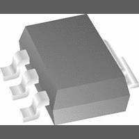
LM1117MP-2.5 National Semiconductor, LM1117MP-2.5 Datasheet - Page 11

LM1117MP-2.5
Manufacturer Part Number
LM1117MP-2.5
Description
Linear Voltage Regulator IC
Manufacturer
National Semiconductor
Datasheet
1.LM1117MP-2.5.pdf
(21 pages)
Specifications of LM1117MP-2.5
No. Of Pins
4
Output Current
0.8A
Mounting Type
Surface Mount
Voltage Regulator Type
LDO Linear
Peak Reflow Compatible (260 C)
No
Supply Voltage
15V
Current Rating
800A
Output Voltage Max
2.5V
Lead Free Status / RoHS Status
Contains lead / RoHS non-compliant
Available stocks
Company
Part Number
Manufacturer
Quantity
Price
Company:
Part Number:
LM1117MP-2.5
Manufacturer:
NSC
Quantity:
512
Part Number:
LM1117MP-2.5
Manufacturer:
NSC
Quantity:
20 000
Part Number:
LM1117MP-2.5/NOPB
Manufacturer:
NS/国半
Quantity:
20 000
Application Note
The LM1117 regulators have internal thermal shutdown to
protect the device from over-heating. Under all possible
operating conditions, the junction temperature of the LM1117
must be within the range of 0˚C to 125˚C. A heatsink may be
required depending on the maximum power dissipation and
maximum ambient temperature of the application. To deter-
mine if a heatsink is needed, the power dissipated by the
regulator, P
Figure 6 shows the voltages and currents which are present
in the circuit.
Mounted on a printed circuit board. Note that the case
temperature is measured at the point where the leads
FIGURE 5. Cross-sectional view of Integrated Circuit
I
P
IN
D
= I
= (V
L
Layout
contact with the mounting pad surface
FIGURE 6. Power Dissipation Diagram
+ I
IN
10
12
13
11
D
-V
1
2
3
4
5
6
7
8
9
G
, must be calculated:
OUT
)I
L
+ V
IN
I
G
Top Side (in
(Continued)
0.0123
0.066
0.066
0.175
0.53
0.76
0.3
1
0
0
0
0
0
2
Copper Area
)*
TABLE 1. θ
10091916
Bottom Side (in
10091937
JA
Different Heatsink Area
0.066
0.175
0.2
0.4
0.6
0.8
0
0
0
0
0
0
1
11
The next parameter which must be calculated is the maxi-
mum allowable temperature rise, T
where T
ture (125˚C), and T
perature which will be encountered in the application.
Using the calculated values for T
mum allowable value for the junction-to-ambient thermal
resistance (θ
If the maximum allowable value for θ
≥136˚C/W for SOT-223 package or ≥79˚C/W for TO-220
package or ≥92˚C/W for TO-252 package, no heatsink is
needed since the package alone will dissipate enough heat
to satisfy these requirements. If the calculated value for θ
falls below these limits, a heatsink is required.
As a design aid, Table 1 shows the value of the θ
SOT-223 and TO-252 for different heatsink area. The copper
patterns that we used to measure these θ
the end of the Application Notes Section. Figure 7 and Figure
8 reflects the same test results as what are in the Table 1
Figure 9 and Figure 10 shows the maximum allowable power
dissipation vs. ambient temperature for the SOT-223 and
TO-252 device. Figures Figure 11 and Figure 12 shows the
maximum allowable power dissipation vs. copper area (in
for the SOT-223 and TO-252 devices. Please see AN1028
for power enhancement techniques to be used with SOT-223
and TO-252 packages.
*Application Note AN-1187 discusses improved thermal per-
formance and power dissipation for the LLP.
2
)
T
θ
JA
R
(max) = T
= T
J
(max) is the maximum allowable junction tempera-
(θ
R
(max)/P
JA
JA
,˚C/W) SOT-223
J
) can be calculated:
(max)-T
136
123
115
125
84
75
69
66
98
89
82
79
93
D
A
(max) is the maximum ambient tem-
Thermal Resistance
A
(max)
R
(max) and P
R
(max):
(θ
JA
,˚C/W) TO-252
JA
JA
103
is found to be
s are shown at
87
60
54
52
47
84
70
63
57
57
89
72
D
www.national.com
, the maxi-
JA
JA
of
2
)


