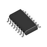
DS34LV86TM National Semiconductor, DS34LV86TM Datasheet - Page 3

DS34LV86TM
Manufacturer Part Number
DS34LV86TM
Description
Line Receiver IC
Manufacturer
National Semiconductor
Datasheet
1.DS34LV86TM.pdf
(10 pages)
Specifications of DS34LV86TM
Driver Case Style
NSOIC
No. Of Pins
16
No. Of Driver/receivers
0/1
Peak Reflow Compatible (260 C)
No
Supply Voltage
3.3V
Current Rating
25A
Supply Voltage Max
3.3V
Leaded Process Compatible
No
Interface Circuit Standard 1
EIA/TIA-422-B/RS-422
Number Of Receivers
4
Number Of Transmitters
Not Required
Number Of Transceivers
Not Required
Data Transmission Topology
Multidrop
Receiver Signal Type
Differential
Transmitter Signal Type
Not Required
Single Supply Voltage (typ)
3.3V
Single Supply Voltage (min)
3V
Single Supply Voltage (max)
3.6V
Dual Supply Voltage (typ)
Not RequiredV
Dual Supply Voltage (min)
Not RequiredV
Dual Supply Voltage (max)
Not RequiredV
Supply Current
15mA
Power Supply Requirement
Single
Operating Temp Range
-40C to 85C
Operating Temperature Classification
Industrial
Mounting
Surface Mount
Pin Count
16
Package Type
SOIC N
Lead Free Status / RoHS Status
Contains lead / RoHS non-compliant
Lead Free Status / RoHS Status
Contains lead / RoHS non-compliant
Available stocks
Company
Part Number
Manufacturer
Quantity
Price
Company:
Part Number:
DS34LV86TM
Manufacturer:
national
Quantity:
2 175
Part Number:
DS34LV86TM
Manufacturer:
NS/国半
Quantity:
20 000
Company:
Part Number:
DS34LV86TM/NOPB
Manufacturer:
NS
Quantity:
96
Part Number:
DS34LV86TM/NOPB
Manufacturer:
NS
Quantity:
20 000
Part Number:
DS34LV86TMX
Manufacturer:
NS/国半
Quantity:
20 000
t
t
t
t
t
t
t
t
t
t
t
f
PHL
PLH
r
f
PHZ
PLZ
PZH
PZL
SK1
SK2
SK3
MAX
Switching Characteristics
Over Supply Voltage and Operating Temperature ranges, unless otherwise specified.
Note 1: “Absolute Maximum Ratings” are those values beyond which the safety of the device cannot be guaranteed. They are not meant to imply that the devices
should be operated at these limits. The table of “Electrical Characteristics” specifies conditions of device operation.
Note 2: Current into device pins is defined as positive. Current out of device pins is defined as negative. All voltages are referenced to ground except V
Note 3: All typicals are given for: V
Note 4: Short one output at a time to ground. Do not exceed package power dissipation ratings.
Note 5: t
Note 6: t
Note 7: t
±0.1V of one another,and a Delta T
characterization.
Note 8: All channels switching, output duty cycle criteria is 40%/60% measured at 50% Input = 1V to 2V, 50% Duty Cycle, t
by design and characterization.
Parameter Measurement Information
Symbol
SK1
SK2
SK3
is the |t
is the maximum skew between any two channels within a device, on either edge.
is the difference in propagation delay times between any channels of any devices. This specification (maximum limit) applies to devices within V
Propagation Delay High to Low
Propagation DeIay Low to High
Rise Time (20% to 80%)
Fall Time (80% to 20%)
Disable Time
Disable Time
Enable Time
Enable Time
Skew, |t
Skew, Pin to Pin (Note 6)
Skew, Part to Part (Note 7)
Maximum Operating Frequency
(Note 8)
PHL
FIGURE 1. Receiver Propagation Delay and Transition Time Test Circuit (Notes 9, 10)
− t
PHL
PLH
| of a channel.
− t
PLH
Parameter
CC
A
= ±5°C (between devices) within the operating temperature range. This parameter is guaranteed by design and
|(Note 5)
= +3.3V, T
A
= +25°C.
(Notes 3, 9, 10)
C
(Figures 1, 2 )
C
(Figures 3, 4)
C
C
L
L
L
L
= 15 pF
= 50 pF
= 15 pF
= 15 pF
Conditions
3
Min
32
6
6
17.5
17.8
Typ
1264402
r
4.1
3.3
0.3
0.6
/t
7
f
≤
5 ns. This parameter is guaranteed
Max
35
35
10
10
40
40
40
40
17
4
4
www.national.com
Units
MHz
ID
ns
ns
ns
ns
ns
ns
ns
ns
ns
ns
ns
.
CC


