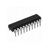
DAC0832LCN National Semiconductor, DAC0832LCN Datasheet - Page 7

DAC0832LCN
Manufacturer Part Number
DAC0832LCN
Description
D/A Converter (D-A) IC
Manufacturer
National Semiconductor
Datasheet
1.DAC0832LCN.pdf
(28 pages)
Specifications of DAC0832LCN
Resolution (bits)
8bit
Data Interface
CMOS, Parallel, TTL
No. Of Pins
20
Settling Time
1µs
Mounting Type
Through Hole
Peak Reflow Compatible (260 C)
No
No. Of Bits
8 Bit
Leaded Process Compatible
No
Number Of Channels
1
Resolution
8b
Interface Type
Parallel
Single Supply Voltage (typ)
Not RequiredV
Dual Supply Voltage (typ)
Not RequiredV
Architecture
R-2R
Power Supply Requirement
Digital
Output Type
Current
Integral Nonlinearity Error
0.2LSB
Single Supply Voltage (min)
Not RequiredV
Single Supply Voltage (max)
Not RequiredV
Dual Supply Voltage (min)
Not RequiredV
Dual Supply Voltage (max)
Not RequiredV
Operating Temp Range
0C to 70C
Operating Temperature Classification
Commercial
Mounting
Through Hole
Pin Count
20
Package Type
PDIP
Lead Free Status / RoHS Status
Contains lead / RoHS non-compliant
Lead Free Status / RoHS Status
Contains lead / RoHS non-compliant
Available stocks
Company
Part Number
Manufacturer
Quantity
Price
Company:
Part Number:
DAC0832LCN
Manufacturer:
NS
Quantity:
6 000
Company:
Part Number:
DAC0832LCN
Manufacturer:
NS
Quantity:
6 000
Part Number:
DAC0832LCN
Manufacturer:
NS/国半
Quantity:
20 000
Definition of Package Pinouts
Control Signals
CS:
ILE:
WR
WR
XFER: Transfer control signal (active low). The XFER will
Other Pin Functions
DI
I
I
R
Linearity Error
Definition of Terms
Resolution: Resolution is directly related to the number of
switches or bits within the DAC. For example, the DAC0830
has 2
Linearity Error: Linearity Error is the maximum deviation
from a straight line passing through the endpoints of the
DAC transfer characteristic . It is measured after adjusting for
zero and full-scale. Linearity error is a parameter intrinsic to
the device and cannot be externally adjusted.
National’s linearity “end point test” (a) and the “best straight
line” test (b,c) used by other suppliers are illustrated above.
The “end point test’’ greatly simplifies the adjustment proce-
dure by eliminating the need for multiple iterations of check-
ing the linearity and then adjusting full scale until the linearity
is met. The “end point test’’ guarantees that linearity is met
OUT1
OUT2
fb
(All control signals level actuated)
a) End point test afterzero and fs
0
-DI
:
1
2
:
:
:
:
8
7
: Digital Inputs. DI
or 256 steps and therefore has 8-bit resolution.
Chip Select (active low). The CS in combination
with ILE will enable WR
Input Latch Enable (active high). The ILE in com-
bination with CS enables WR
Write 1. The active low WR
digital input data bits (DI) into the input latch. The
data in the input latch is latched when WR
To update the input latch–CS and WR
while ILE is high.
Write 2 (active low). This signal, in combination with
XFER, causes the 8-bit data which is available in the
input latch to transfer to the DAC register.
enable WR
and DI
DAC Current Output 1. I
digital code of all 1’s in the DAC register, and is
zero for all 0’s in DAC register.
DAC Current Output 2. I
I
fixed reference voltage).
Feedback Resistor. The feedback resistor is pro-
vided on the IC chip for use as the shunt feedback
OUT1
, or I
7
is the most significant bit (MSB).
adj.
2
OUT1
.
+ I
0
OUT2
is the least significant bit (LSB)
00560823
1
.
= constant (I full scale for a
OUT1
OUT2
1
1
.
is used to load the
is a constant minus
is a maximum for a
1
must be low
1
is high.
b) Best straight line
7
V
V
GND:
For example, if V
I
Pin 3 can be offset
logic input threshold will shift.
after a single full scale adjust. (One adjustment vs. multiple
iterations of the adjustment.) The “end point test’’ uses a
standard zero and F.S. adjustment procedure and is a much
more stringent test for DAC linearity.
Power Supply Sensitivity: Power supply sensitivity is a
measure of the effect of power supply changes on the DAC
full-scale output.
Settling Time: Settling time is the time required from a code
transition until the DAC output reaches within
final output value. Full-scale settling time requires a zero to
full-scale or full-scale to zero output change.
Full Scale Error: Full scale error is a measure of the output
error between an ideal DAC and the actual device output.
OUT1
REF
CC
:
:
00560824
and I
resistor for the external op amp which is used to
provide an output voltage for the DAC. This on-chip
resistor should always be used (not an external
resistor) since it matches the resistors which are
used in the on-chip R-2R ladder and tracks these
resistors over temperature.
Reference Voltage Input. This input connects an
external precision voltage source to the internal
R-2R ladder. V
of +10 to −10V. This is also the analog voltage input
for a 4-quadrant multiplying DAC application.
Digital Supply Voltage. This is the power supply
pin for the part. V
Operation is optimum for +15V
The pin 10 voltage must be at the same ground
potential as I
applications. Any difference of potential (V
10) will result in a linearity change of
OUT2
the linearity change will be 0.03%.
REF
±
100mV with no linearity change, but the
= 10V and pin 10 is 9mV offset from
OUT1
REF
c) Shifting fs adj. to pass
CC
and I
best straight line test
can be selected over the range
can be from +5 to +15V
OUT2
for current switching
DC
±
00560825
1
⁄
2
www.national.com
LSB of the
OS
DC
pin
.


