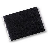
SST39VF1681-70-4C-EKE SILICON STORAGE TECHNOLOGY, SST39VF1681-70-4C-EKE Datasheet - Page 4

SST39VF1681-70-4C-EKE
Manufacturer Part Number
SST39VF1681-70-4C-EKE
Description
IC, 16M FLASH MEMORY, 2KWORD SECTOR
Manufacturer
SILICON STORAGE TECHNOLOGY
Datasheet
1.SST39VF1681-70-4C-EKE.pdf
(29 pages)
Specifications of SST39VF1681-70-4C-EKE
Memory Size
16Mbit
Supply Voltage Range
2.7V To 3.6V
Memory Case Style
TSOP
No. Of Pins
48
Svhc
No SVHC (18-Jun-2010)
Access Time
70ns
Interface
X8 MPF+
Memory Configuration
2M X 8bit
Memory Type
Flash - NOR
Interface Type
CFI
Rohs Compliant
Yes
Lead Free Status / RoHS Status
Lead free / RoHS Compliant
Available stocks
Company
Part Number
Manufacturer
Quantity
Price
Company:
Part Number:
SST39VF1681-70-4C-EKE
Manufacturer:
SST
Quantity:
106
Preliminary Specifications
Data Protection
The SST39VF168x provide both hardware and software
features to protect nonvolatile data from inadvertent writes.
Hardware Data Protection
Noise/Glitch Protection: A WE# or CE# pulse of less than 5
ns will not initiate a write cycle.
V
inhibited when V
Write Inhibit Mode: Forcing OE# low, CE# high, or WE#
high will inhibit the Write operation. This prevents inadvert-
ent writes during power-up or power-down.
Hardware Block Protection
The SST39VF1682 supports top hardware block protec-
tion, which protects the top 64 KByte block of the device.
The SST39VF1681 supports bottom hardware block pro-
tection, which protects the bottom 64 KByte block of the
device. The Boot Block address ranges are described in
Table 2. Program and Erase operations are prevented on
the 64 KByte when WP# is low. If WP# is left floating, it is
internally held high via a pull-up resistor, and the Boot
Block is unprotected, enabling Program and Erase opera-
tions on that block.
TABLE 2: B
©2003 Silicon Storage Technology, Inc.
Product
Bottom Boot Block
Top Boot Block
DD
SST39VF1681
SST39VF1682
Power Up/Down Detection: The Write operation is
OOT
DD
is less than 1.5V.
B
LOCK
A
DDRESS
1F0000H-1FFFFFH
000000H-00FFFFH
Address Range
R
ANGES
T2.1 1243
4
Hardware Reset (RST#)
The RST# pin provides a hardware method of resetting the
device to read array data. When the RST# pin is held low
for at least T
return to Read mode. When no internal Program/Erase
operation is in progress, a minimum period of T
required after RST# is driven high before a valid Read can
take place (see Figure 15).
The Erase or Program operation that has been interrupted
needs to be reinitiated after the device resumes normal
operation mode to ensure data integrity.
Software Data Protection (SDP)
The SST39VF168x provide the JEDEC approved Software
Data Protection scheme for all data alteration operations,
i.e., Program and Erase. Any Program operation requires
the inclusion of the three-byte sequence. The three-byte
load sequence is used to initiate the Program operation,
providing optimal protection from inadvertent Write opera-
tions, e.g., during the system power-up or power-down.
Any Erase operation requires the inclusion of six-byte
sequence. These devices are shipped with the Software
Data Protection permanently enabled. See Table 6 for the
specific software command codes. During SDP command
sequence, invalid commands will abort the device to Read
mode within T
Common Flash Memory Interface (CFI)
The SST39VF168x also contain the CFI information to
describe the characteristics of the device. In order to enter
the CFI Query mode, the system must write three-byte
sequence, same as product ID entry command with 98H
(CFI Query command) to address AAAH in the last byte
sequence. Once the device enters the CFI Query mode, the
system can read CFI data at the addresses given in Tables
7 through 9. The system must write the CFI Exit command
to return to Read mode from the CFI Query mode.
16 Mbit Multi-Purpose Flash Plus
RP ,
RC.
SST39VF1681 / SST39VF1682
any in-progress operation will terminate and
S71243-03-000
RHR
11/03
is


