SST39VF010-70-4I-NHE SILICON STORAGE TECHNOLOGY, SST39VF010-70-4I-NHE Datasheet - Page 6
SST39VF010-70-4I-NHE
Manufacturer Part Number
SST39VF010-70-4I-NHE
Description
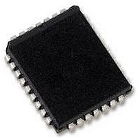
MEMORY, FLASH, 1MBIT, PARL, 32PLCC
Manufacturer
SILICON STORAGE TECHNOLOGY
Datasheet
1.SST39VF512-70-4C-NHE.pdf
(24 pages)
Specifications of SST39VF010-70-4I-NHE
Memory Size
1Mbit
Supply Voltage Range
2.7V To 3.6V
Memory Case Style
LCC
No. Of Pins
32
Operating Temperature Range
-40°C To +85°C
Svhc
No SVHC (18-Jun-2010)
Access Time
70ns
Interface
X8
Memory Type
Flash - NOR
Memory Configuration
128K X 8
Rohs Compliant
Yes
Lead Free Status / RoHS Status
Lead free / RoHS Compliant
Available stocks
Company
Part Number
Manufacturer
Quantity
Price
Company:

Part Number:
SST39VF010-70-4I-NHE
Manufacturer:
Microchip Technology
Quantity:
10 000
Part Number:
SST39VF010-70-4I-NHE
Manufacturer:
SST
Quantity:
20 000
Company:
Part Number:
SST39VF010-70-4I-NHE-T
Manufacturer:
Microchip Technology
Quantity:
10 000


Data Sheet
TABLE 2: Pin Description
TABLE 3: Operation Modes Selection
©2010 Silicon Storage Technology, Inc.
Symbol
A
DQ
CE#
OE#
WE#
V
V
NC
Mode
Read
Program
Erase
Standby
Write Inhibit
Product Identification
Software Mode
MS
DD
SS
FIGURE 5: Pin Assignment for 34-ball WFBGA (4mm x 6mm) for 1 Mbit and 2 Mbit
1. A
1. X can be V
7
1
-DQ
-A
A
MS
MS
0
0
= Most significant address
= A
15
for SST39LF/VF512, A
Pin Name
Address Inputs
Data Input/output
Chip Enable
Output Enable
Write Enable
Power Supply
Ground
No Connection
IL
or V
IH
, but no other value.
6
5
4
3
2
1
16
Functions
To provide memory addresses. During Sector-Erase A
sector. During Block-Erase A
To output data during Read cycles and receive input data during Write cycles.
Data is internally latched during a Write cycle.
The outputs are in tri-state when OE# or CE# is high.
To activate the device when CE# is low.
To gate the data output buffers.
To control the Write operations.
To provide power supply voltage:
Unconnected pins.
for SST39LF/VF010, A
CE#
V
SST39VF512 / SST39VF010 / SST39VF020 / SST39VF040
V
V
V
V
CE#
V
SST39LF512 / SST39LF010 / SST39LF020 / SST39LF040
A2
A1
A0
X
X
SS
IH
IL
IL
IL
IL
512 Kbit / 1 Mbit / 2 Mbit / 4 Mbit Multi-Purpose Flash
V
A17
A16
A12
A
DD
Note: For SST39LF020, ball B3 is "No Connect"
WE#
A14
A18
A15
A8
A6
B
OE#
V
V
V
V
V
X
X
IH
IH
IL
IL
IL
TOP VIEW (balls facing down)
For SST39LF010, balls B3 and A5 are "No Connect"
A13
C
A9
A7
A5
A11
A4
D
17
for SST39LF/VF020, and A
WE#
V
V
V
V
V
NC1
NC2
X
X
E
6
IH
IL
IL
IH
IH
MS
OE#
A3
F
-A
DQ
D
D
X
High Z
High Z/ D
High Z/ D
DQ7
16
A10
G
1
A0
A2
OUT
IN
address lines will select the block.
3.0-3.6V for SST39LF512/010/020/040
2.7-3.6V for SST39VF512/010/020/040
CE#
DQ5
DQ3
DQ2
DQ0
H
A1
OUT
OUT
DQ6
DQ4
DQ1
V
J
SS
18
for SST39LF/VF040
MS
-A
Address
A
A
Sector address,
XXH for Chip-Erase
X
X
X
See Table 4
IN
IN
12
address lines will select the
S71150-14-000
T2.1 1150
T3.4 1150
01/10
Related parts for SST39VF010-70-4I-NHE
Image
Part Number
Description
Manufacturer
Datasheet
Request
R

Part Number:
Description:
512 Kbit/1 Mbit (x8) multi-purpose flash
Manufacturer:
Silicon Storage Technology, Inc
Datasheet:
Part Number:
Description:
512 Kbit/1 Mbit (x8) multi-purpose flash
Manufacturer:
Silicon Storage Technology, Inc
Datasheet:
Part Number:
Description:
Manufacturer:
Silicon Storage Technology, Inc
Datasheet:
Part Number:
Description:
Manufacturer:
Silicon Storage Technology, Inc
Datasheet:

Part Number:
Description:
1M FLASH MEMORY, 4KB SECTOR, TSOP32
Manufacturer:
SILICON STORAGE TECHNOLOGY
Datasheet:
Part Number:
Description:
MEMORY, FLASH, 1MBIT, PARL, 32TSOP
Manufacturer:
SILICON STORAGE TECHNOLOGY
Datasheet:
Part Number:
Description:
4 Mbit firmware hub
Manufacturer:
Silicon Storage Technology, Inc
Datasheet:
Part Number:
Description:
Manufacturer:
Silicon Storage Technology, Inc
Datasheet:
Part Number:
Description:
1 Mbit (128K x 8) page-mode EEPROM
Manufacturer:
Silicon Storage Technology, Inc
Datasheet:
Part Number:
Description:
1 Mbit (128K x 8) page-mode EEPROM
Manufacturer:
Silicon Storage Technology, Inc
Datasheet:
Part Number:
Description:
2 Mbit (256K x 8) page-mode EEPROM
Manufacturer:
Silicon Storage Technology, Inc
Datasheet: