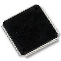
LFXP3C-5TN144C LATTICE SEMICONDUCTOR, LFXP3C-5TN144C Datasheet - Page 56

LFXP3C-5TN144C
Manufacturer Part Number
LFXP3C-5TN144C
Description
FPGA, 1.8V FLASH, INSTANT ON, SMD
Manufacturer
LATTICE SEMICONDUCTOR
Series
LatticeXPr
Datasheet
1.LFXP3C-3QN208C.pdf
(130 pages)
Specifications of LFXP3C-5TN144C
No. Of Logic Blocks
384
No. Of Macrocells
1500
Family Type
LatticeXP
No. Of Speed Grades
5
No. Of I/o's
100
Clock Management
PLL
Core Supply Voltage Range
1.71V To 3.465V
Lead Free Status / RoHS Status
Lead free / RoHS Compliant
Available stocks
Company
Part Number
Manufacturer
Quantity
Price
Company:
Part Number:
LFXP3C-5TN144C
Manufacturer:
Lattice
Quantity:
17
Company:
Part Number:
LFXP3C-5TN144C
Manufacturer:
Lattice Semiconductor Corporation
Quantity:
10 000
Lattice Semiconductor
sysCLOCK PLL Timing
LatticeXP “C” Sleep Mode Timing
f
f
f
f
f
AC Characteristics
t
t
t
t
t
t
t
t
t
t
t
t
1. Jitter sample is taken over 10,000 samples of the primary PLL output with clean reference clock.
2. Output clock is valid after t
3. Using LVDS output buffers.
4. As compared to CLKOP output.
Timing v.F0.11
t
t
t
t
IN
OUT
OUT2
VCO
PFD
DT
PH
OPJIT
SK
W
LOCK
PA
IPJIT
FBKDLY
HI
LO
RST
PWRDN
PWRUP
WSLEEPN
WAWAKE
Parameter
Parameter
4
2
1
Input Clock Frequency (CLKI, CLKFB)
Output Clock Frequency (CLKOP, CLKOS)
K-Divider Output Frequency (CLKOK)
PLL VCO Frequency
Phase Detector Input Frequency
Output Clock Duty Cycle
Output Phase Accuracy
Output Clock Period Jitter
Input Clock to Output Clock Skew
Output Clock Pulse Width
PLL Lock-in Time
Programmable Delay Unit
Input Clock Period Jitter
External Feedback Delay
Input Clock High Time
Input Clock Low Time
RST Pulse Width
SLEEPN
SLEEPN Low to I/O Tristate
SLEEPN High to Power Up
SLEEPN Pulse Width to Initiate Sleep Mode
SLEEPN Pulse Rejection
I/O
LOCK
Descriptions
for PLL reset and dynamic delay adjustment.
Over Recommended Operating Conditions
Descriptions
t
PWRDN
LFXP3
LFXP6
LFXP10
LFXP15
LFXP20
Default duty cycle elected
f
f
Divider ratio = integer
At 90% or 10%
90% to 90%
10% to 10%
OUT
OUT
3-25
Š 100MHz
< 100MHz
Conditions
3
Sleep Mode
Min.
400
—
—
—
—
—
—
—
DC and Switching Characteristics
3
LatticeXP Family Data Sheet
t
PWRUP
Typ.
1.1
1.4
1.7
1.4
1.7
20
—
—
0.195
Min.
375
100
0.5
0.5
25
25
25
45
10
—
—
—
—
—
—
—
1
Typ.
250
50
—
—
—
—
—
—
—
—
—
—
—
—
—
—
—
—
Max.
120
2.1
2.4
1.8
2.1
2.4
32
—
+/- 125
+/- 200
+/- 200
187.5
Max.
0.05
0.02
375
375
750
150
400
55
10
—
—
—
—
—
Units
ms
ms
ms
ms
ms
ns
ns
ns
Units
UIPP
MHz
MHz
MHz
MHz
MHz
UI
ps
ps
ns
us
ps
ps
ns
ns
ns
ns
%


