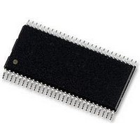
DS90CR287MTD National Semiconductor, DS90CR287MTD Datasheet - Page 11

DS90CR287MTD
Manufacturer Part Number
DS90CR287MTD
Description
IC, TRANSMITTER LVDS 85MHZ, 90CR287
Manufacturer
National Semiconductor
Datasheet
1.DS90CR287MTD.pdf
(16 pages)
Specifications of DS90CR287MTD
Device Type
Line
Supply Current Max
135mA
Peak-to-peak Jitter Max
2ns
Signal Input Type
LVCMOS, LVTTL
Output Level Type
LVDS
Supply Voltage Range
3V To 3.6V
Esd Hbm
7kV
Operating
RoHS Compliant
Signaling Rate
2.38Gbps
Rohs Compliant
Yes
Available stocks
Company
Part Number
Manufacturer
Quantity
Price
Company:
Part Number:
DS90CR287MTD
Manufacturer:
NS
Quantity:
216
Company:
Part Number:
DS90CR287MTD/NOPB
Manufacturer:
PIONEER
Quantity:
560
Part Number:
DS90CR287MTDX
Manufacturer:
NS/国半
Quantity:
20 000
Company:
Part Number:
DS90CR287MTDX/NOPB
Manufacturer:
TI
Quantity:
1 600
Company:
Part Number:
DS90CR287MTDX/NOPB
Manufacturer:
NSC
Quantity:
83
TxIN
TxOUT+
TxOUT−
TxCLK IN
TxCLK OUT+
TxCLK OUT−
PWR DOWN
V
GND
PLL V
PLL GND
LVDS V
LVDS GND
RxIN+
RxIN−
RxOUT
RxCLK IN+
RxCLK IN−
RxCLK OUT
PWR DOWN
V
AC Timing Diagrams
C — Setup and Hold Time (Internal data sampling window) defined by Rspos (receiver input strobe position) min and max
Tppos — Transmitter output pulse position (min and max)
RSKM ≥ Cable Skew (type, length) + Source Clock Jitter (cycle to cycle)(Note 7) + ISI (Inter-symbol interference)(Note 8)
Cable Skew — typically 10 ps–40 ps per foot, media dependent
Note 7: Cycle-to-cycle jitter is less than 150ps at 85MHz.
Note 8: ISI is dependent on interconnect length; may be zero
DS90CR287 MTD56 (TSSOP) Package Pin Description — Channel Link
Transmitter
DS90CR288A MTD56 (TSSOP) Package Pin Description — Channel Link
Receiver
CC
CC
Pin Name
Pin Name
CC
CC
I/O
I/O
O
O
O
O
O
O
I
I
I
I
I
I
I
I
I
I
I
I
I
I
I
No.
No.
28
28
4
4
1
1
1
1
4
5
1
2
1
3
4
4
1
1
1
1
4
TTL level input.
Positive LVDS differential data output.
Negative LVDS differential data output.
TTL level clock input. The rising edge acts as data strobe. Pin name TxCLK IN. See
Applications Information section.
Positive LVDS differential clock output.
Negative LVDS differential clock output.
TTL level input. Assertion (low input) TRI-STATES the outputs, ensuring low current at
power down. See Applications Information section.
Power supply pins for TTL inputs.
Ground pins for TTL inputs.
Power supply pin for PLL.
Ground pins for PLL.
Power supply pin for LVDS outputs.
Ground pins for LVDS outputs.
Positive LVDS differential data inputs.
Negative LVDS differential data inputs.
TTL level data outputs.
Positive LVDS differential clock input.
Negative LVDS differential clock input.
TTL level clock output. The rising edge acts as data strobe. Pin name RxCLK OUT.
TTL level input. When asserted (low input) the receiver outputs are low.
Power supply pins for TTL outputs.
(Continued)
FIGURE 16. Receiver LVDS Input Skew Margin
11
Description
Description
10108720
www.national.com


