ADG528AKPZ Analog Devices Inc, ADG528AKPZ Datasheet - Page 6
ADG528AKPZ
Manufacturer Part Number
ADG528AKPZ
Description
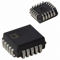
IC, ANALOG MULTIPLEXER, 8 X 1, LCC-20
Manufacturer
Analog Devices Inc
Type
Analog Multiplexerr
Datasheet
1.ADG529AKNZ.pdf
(12 pages)
Specifications of ADG528AKPZ
No. Of Circuits
1
Supply Current
600µA
On State Resistance Max
280ohm
Supply Voltage Range
10.8V To 16.5V
Operating Temperature Range
-40°C To +85°C
Analog Switch Case Style
LCC
Function
Multiplexer
Circuit
1 x 8:1
On-state Resistance
300 Ohm
Voltage Supply Source
Dual Supply
Voltage - Supply, Single/dual (±)
±10.8 V ~ 16.5 V
Current - Supply
20µA
Operating Temperature
-40°C ~ 85°C
Mounting Type
Surface Mount
Package / Case
20-LCC (J-Lead)
Multiplexer Configuration
Single 8:1
Number Of Inputs
8
Number Of Outputs
1
Number Of Channels
1
Analog Switch On Resistance
700@16.5VOhm
Analog Switch Turn On Time
450ns
Analog Switch Turn Off Time
450ns
Package Type
PLCC
Power Supply Requirement
Single/Dual
Single Supply Voltage (min)
10.8V
Single Supply Voltage (typ)
12/15V
Single Supply Voltage (max)
16.5V
Dual Supply Voltage (min)
±10.8V
Dual Supply Voltage (typ)
±12/±15V
Dual Supply Voltage (max)
±16.5V
Power Dissipation
470mW
Mounting
Surface Mount
Pin Count
20
Operating Temp Range
-40C to 85C
Operating Temperature Classification
Industrial
Lead Free Status / RoHS Status
Lead free / RoHS Compliant
Lead Free Status / RoHS Status
Lead free / RoHS Compliant, Lead free / RoHS Compliant
Available stocks
Company
Part Number
Manufacturer
Quantity
Price
Company:

Part Number:
ADG528AKPZ
Manufacturer:
TI
Quantity:
257
Company:
Part Number:
ADG528AKPZ
Manufacturer:
Analog Devices Inc
Quantity:
10 000
Part Number:
ADG528AKPZ
Manufacturer:
ADI/亚德诺
Quantity:
20 000
Company:
Part Number:
ADG528AKPZ-REEL
Manufacturer:
Analog Devices Inc
Quantity:
10 000


ADG528A/ADG529A
A2 A1 A0 EN WR RS ON SWITCH PAIR
X
X
X
0
0
0
0
1
1
1
1
X = Don’t Care
A1 A0 EN WR RS ON SWITCH PAIR
X
X
X
0
0
1
1
X = Don’t Care
X
X
X
0
0
1
1
0
0
1
1
X
X
X
0
1
0
1
X
X
X
0
1
0
1
0
1
0
1
X
X
0
1
1
1
1
X
X
0
1
1
1
1
1
1
1
1
X
0
0
0
0
0
X
0
0
0
0
0
0
0
0
0
1
0
1
1
1
1
1
TRUTH TABLES
1
0
1
1
1
1
1
1
1
1
1
ADG529A
Retains Previous Switch Condition
NONE (Address and Enable Latches
Cleared)
NONE
1
2
3
4
Retains Previous Switch Condition
NONE (Address and Enable
Latches Cleared)
NONE
1
2
3
4
5
6
7
8
ADG528A
–6–
Figure 1 shows the timing sequence for latching the switch
address and enable inputs. The latches are level sensitive; there-
fore, while WR is held low, the latches are transparent and the
switches respond to the address and enable inputs. This input
data is latched on the rising edge of WR.
Figure 2 shows the Reset Pulse Width, t
Time, t
Note: All digital input signals rise and fall times measured from
10% to 90% of 3 V. t
OFF
(RS).
TIMING DIAGRAMS
R
= t
F
Figure 1.
Figure 2.
= 20 ns.
RS
, and Reset Turn-off
REV. B
Related parts for ADG528AKPZ
Image
Part Number
Description
Manufacturer
Datasheet
Request
R

Part Number:
Description:
±1.7g Dual-Axis IMEMS Accelerometer Evaluation Board
Manufacturer:
Analog Devices Inc
Datasheet:

Part Number:
Description:
Inertial Sensor Evaluation System
Manufacturer:
Analog Devices Inc
Datasheet:
Part Number:
Description:
Manufacturer:
Analog Devices Inc
Datasheet:
Part Number:
Description:
Manufacturer:
Analog Devices Inc
Datasheet:
Part Number:
Description:
Manufacturer:
Analog Devices Inc
Datasheet:
Part Number:
Description:
Manufacturer:
Analog Devices Inc
Datasheet:
Part Number:
Description:
Manufacturer:
Analog Devices Inc
Datasheet:
Part Number:
Description:
Manufacturer:
Analog Devices Inc
Datasheet:
Part Number:
Description:
Manufacturer:
Analog Devices Inc
Datasheet:
Part Number:
Description:
Manufacturer:
Analog Devices Inc
Datasheet:
Part Number:
Description:
Manufacturer:
Analog Devices Inc
Datasheet:
Part Number:
Description:
Manufacturer:
Analog Devices Inc
Datasheet:
Part Number:
Description:
Manufacturer:
Analog Devices Inc
Datasheet: