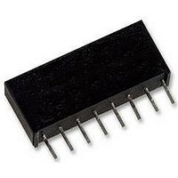
THAT2181AL08-U THAT Corporation, THAT2181AL08-U Datasheet - Page 7

THAT2181AL08-U
Manufacturer Part Number
THAT2181AL08-U
Description
AMP, VOLT CONTROLLED, TRIMMABLE, 2181
Manufacturer
THAT Corporation
Datasheet
1.THAT2181AL08-U.pdf
(12 pages)
Specifications of THAT2181AL08-U
Brief Features
Exponential Gain Control, Wide Gain Range
Supply Voltage Range
± 4V To ± 18V
Operating Temperature Range
0°C To +70°C
Digital Ic Case Style
SIP
No. Of Pins
8
Operating
RoHS Compliant
Ic Function
Voltage Controlled Amplifier
Rohs Compliant
Yes
THAT 2181 Series
Blackmer® Trimmable IC VCAs
Input
currents, not voltages. While this often causes some
conceptual difficulty for designers first exposed to
this convention, the current input/output mode
provides great flexibility in application.
negative feedback provided internally (see Figure 5,
Page 4). The input resistor (shown as 20 kΩ in
Figure 2, Page 3) should be scaled to convert the
available ac input voltage to a current within the
linear range of the device. Generally, peak input
currents should be kept under 1 mA for best distor-
tion performance.
tion varies with signal level for the three parts in the
2181 Series for 0 dB, +15 dB and -15 dB gain. The
circuit of Figure 2, Page 3 was used to generate these
curves.
tion will usually determine the maximum signal
current level which may be used. Note that, with
20 kΩ current-to-voltage converting resistors, distor-
tion remains low even at 10 V rms input at 0 dB or
-15 dB gain, and at 1.7 V rms input at +15 dB gain
(~10 V rms output). This is especially true in the –A
and –B grades of the part.
Distortion vs. Noise
decreasing the 20 kΩ current-to-voltage converting
resistors used at the input and output in Figure 2,
Page 3. For every dB these resistor values are
decreased, the voltage noise at the output of the
OP275 is reduced by one dB. For example, with
10 kΩ resistors, the output noise floor drops to
–104 dBV (typical) at 0 dB gain — a 6 dB reduction
in noise because 10 kΩ is 1/2 of (6 dB lower than)
20 kΩ.
performance, increasing these resistors to 40 kΩ will
increase the noise level by 6 dB, while reducing
distortion at maximum voltage levels. Furthermore, if
maximum signal levels are higher (or lower) than the
traditional 10 V rms, these resistors should be
scaled to accommodate the actual voltages prevalent
in the circuit. Since the 2181 handles signals as
currents, these ICs can even operate with signal
levels far exceeding the 2181's supply rails, provided
appropriately large resistors are used.
As mentioned above, input and output signals are
The Input pin (pin 1) is a virtual ground with
Refer to Figures 10 through 12 to see how distor-
For a specific application, the acceptable distor-
A designer may trade off noise for distortion by
Conversely, if THD is more important than noise
THAT Corporation; 45 Sumner Street; Milford, Massachusetts 01757-1656; USA
Tel: +1 508 478 9200; Fax: +1 508 478 0990; Web: www.thatcorp.com
Copyright © 2008, THAT Corporation
Applications
Page 7 of 12
High-Frequency Distortion
subtle effect on distortion. Since the feedback imped-
ances around the internal opamp (essentially Q1/D1
and Q3/D3) are fixed, low values for the input resis-
tor will require more closed-loop gain from the
opamp. Since the open-loop gain naturally falls off at
high frequencies, asking for too much gain will lead
to increased high-frequency distortion. For best
results, this resistor should be kept to 10 kΩ or
above.
Stability
nal op amp is intended for operation with source
impedances of less than 60 kΩ at high frequencies.
For most audio applications, this will present no
problem.
DC Coupling
input offset voltage) is approximately 0 V, but, as in
many general-purpose opamps, this is not well
controlled. Any dc input currents will cause dc in the
output which will be modulated by gain; this may
cause audible thumps. If the input is dc coupled, dc
input currents may be generated due to the input
offset voltage of the 2181 itself, or due to offsets in
stages preceeding the 2181. Therefore, capacitive
coupling is almost mandatory for quality audio appli-
cations. Choose a capacitor which will give accept-
able low frequency performance for the application.
Summing Multiple Input Signals
resistors, just as with an inverting opamp configura-
tion. In such a case, a single coupling capacitor may
be located next to pin 1 rather than multiple capaci-
tors at the driven ends of the summing resistors.
However, take care that the capacitor does not pick
up stray signals.
Output
connected to a virtual ground node, so that current
flowing in it may be converted to a voltage (see
Figures 2 & 15). Choose the external opamp for good
audio performance. The feedback resistor should be
chosen based on the desired current-to-voltage
conversion constant. Since the input resistor deter-
mines the voltage-to-current conversion at the input,
The choice of input resistor has an additional,
An additional consideration is stability: the inter-
The quiescent dc voltage level at the input (the
Multiple signals may be summed via multiple
The Output pin (pin 8) is intended to be
Document 600030 Rev 02


