LM60CIM3 National Semiconductor, LM60CIM3 Datasheet - Page 3
LM60CIM3
Manufacturer Part Number
LM60CIM3
Description
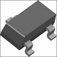
IC, TEMPERATURE SENSOR, ± 3°C, 3-SOT-23
Manufacturer
National Semiconductor
Datasheet
1.LM60BIM3NOPB.pdf
(12 pages)
Specifications of LM60CIM3
Ic Output Type
Voltage
Sensing Accuracy Range
± 3°C
Supply Current
110µA
Supply Voltage Range
2.7V To 10V
Sensor Case Style
SOT-23
No. Of Pins
3
Termination Type
SMD
Filter Terminals
SMD
Rohs Compliant
No
Lead Free Status / RoHS Status
Contains lead / RoHS non-compliant
Available stocks
Company
Part Number
Manufacturer
Quantity
Price

Company:
Part Number:
LM60CIM3
Manufacturer:
TOSHIBA
Quantity:
904
Part Number:
LM60CIM3
Manufacturer:
NS/国半
Quantity:
20 000
Company:
Part Number:
LM60CIM3/NOPB
Manufacturer:
TI
Quantity:
1 001
Company:
Part Number:
LM60CIM3/NOPB
Manufacturer:
NS
Quantity:
1 000
Part Number:
LM60CIM3/NOPB
Manufacturer:
TI/德州仪器
Quantity:
20 000
Company:
Part Number:
LM60CIM3X
Manufacturer:
NS
Quantity:
8 145
Part Number:
LM60CIM3X
Manufacturer:
NS/国半
Quantity:
20 000
Part Number:
LM60CIM3X/NOPB
Manufacturer:
TI/德州仪器
Quantity:
20 000


Accuracy
Output Voltage at 0°C
Nonlinearity
Sensor Gain
(Average Slope)
Output Impedance
Line Regulation
Quiescent Current
Change of Quiescent Current
Temperature Coefficient of
Quiescent Current
Long Term Stability
Absolute Maximum Ratings
Electrical Characteristics
Unless otherwise noted, these specifications apply for +V
T
Note 1: Absolute Maximum Ratings indicate limits beyond which damage to the device may occur. Operating Ratings indicate conditions for which the device is
functional, but do not guarantee specific performance limits. For guaranteed specifications and test conditions, see the Electrical Characteristics. The guaranteed
specifications apply only for the test conditions listed. Some performance characteristics may degrade when the device is not operated under the listed test
conditions.
Note 2: When the input voltage (V
Note 3: The human body model is a 100 pF capacitor discharged through a 1.5 kΩ resistor into each pin. The machine model is a 200 pF capacitor discharged
directly into each pin.
Note 4: Reflow temperature profiles are different for lead-free and non-lead-free packages.
Note 5: The junction to ambient thermal resistance (θ
Note 6: Typicals are at T
Note 7: Limits are guaranteed to National's AOQL (Average Outgoing Quality Level).
Note 8: Accuracy is defined as the error between the output voltage and +6.25 mV/°C times the device's case temperature plus 424 mV, at specified conditions
of voltage, current, and temperature (expressed in °C).
Note 9: Nonlinearity is defined as the deviation of the output-voltage-versus-temperature curve from the best-fit straight line, over the device's rated temperature
range.
Note 10: Regulation is measured at constant junction temperature, using pulse testing with a low duty cycle. Changes in output due to heating effects can be
computed by multiplying the internal dissipation by the thermal resistance.
Supply Voltage
Output Voltage
Output Current
Input Current at any pin
ESD Susceptibility
MIN
Human Body Model
Machine Model
to T
SOT-23
TO-92
(Note
MAX
(Note
Parameter
; all other limits T
8)
(Note
9)
(Note
(Note
J
10)
= T
11)
A
(Note
= 25°C and represent most likely parametric norm.
3) :
I
) at any pin exceeds power supplies (V
A
2)
= T
J
= 25°C.
+3.0V
+2.7V
+2.7V
+2.7V
T
J
1000 hours
=T
MAX
JA
(+V
≤
≤
≤
≤
) is specified without a heat sink in still air.
+12V to −0.2V
Conditions
+V
+V
+V
+V
=+125°C, for
(Note
S
+ 0.6V) to
S
S
S
S
≤
≤
≤
≤
10 mA
2500V
−0.6V
1)
+10V
+3.3V
+10V
+10V
5 mA
250V
200V
S
= +3.0 V
I
< GND or V
3
DC
Operating Ratings
Soldering
Semiconductor's Reflow Temperature Profile specifications.
Refer to www.national.com/packaging.
(Note
Typical
Storage Temperature
Maximum Junction Temperature
(T
Specified Temperature Range:
Supply Voltage Range (+V
Thermal Resistance, θ
+6.25
+424
I
±5.0
±0.2
and I
0.2
> +V
JMAX
LM60B
LM60C
82
SOT-23
TO-92
6)
S
)
), the current at that pin should be limited to 5 mA.
LOAD
= 1 μA. Boldface limits apply for T
process
(Note
LM60B
Limits
+6.06
+6.44
±2.0
±3.0
±0.6
±0.3
±2.3
800
110
125
7)
JA
must
(Note
S
)
(Note
LM60C
(Note
Limits
5)
+6.00
+6.50
±3.0
±4.0
±0.8
±0.3
±2.3
800
110
125
comply
−25°C
−40°C
7)
1)
(Note
T
−65°C to +150°C
MIN
with
≤
≤
+2.7V to +10V
4)
T
T
mV/°C (max)
≤
mV/°C (min)
mV/V (max)
A
A
www.national.com
mV (max)
°C (max)
°C (max)
°C (max)
μA (max)
μA (max)
μA (max)
T
A
Ω (max)
≤
≤
(Limit)
μA/°C
A
450°C/W
180°C/W
Units
= T
mV
+125°C
+125°C
+125°C
National
°C
≤
J
T
=
MAX
Related parts for LM60CIM3
Image
Part Number
Description
Manufacturer
Datasheet
Request
R

Part Number:
Description:
2.7v, Sot-23 Or To-92 Temperature Sensor
Manufacturer:
National Semiconductor Corporation
Datasheet:

Part Number:
Description:
National Semiconductor [8-Bit D/A Converter]
Manufacturer:
National Semiconductor
Datasheet:
Part Number:
Description:
National Semiconductor [Media Coprocessor]
Manufacturer:
National Semiconductor
Datasheet:
Part Number:
Description:
Digitally Controlled Tone and Volume Circuit with Stereo Audio Power Amplifier, Microphone Preamp Stage and National 3D Sound
Manufacturer:
National Semiconductor
Datasheet:
Part Number:
Description:
Digitally Controlled Tone and Volume Circuit with Stereo Audio Power Amplifier, Microphone Preamp Stage and National 3D Sound
Manufacturer:
National Semiconductor
Datasheet:
Part Number:
Description:
AC97 Rev 2 Codec with Sample Rate Conversion and National 3D Sound
Manufacturer:
National Semiconductor
Part Number:
Description:
Manufacturer:
National Semiconductor
Datasheet:
Part Number:
Description:
Manufacturer:
National Semiconductor
Datasheet:
Part Number:
Description:
General Purpose, Low Voltage, Low Power, Rail-to-Rail Output Operational Amplifiers
Manufacturer:
National Semiconductor
Datasheet:
Part Number:
Description:
8-bit 20 MSPS flash A/D converter.
Manufacturer:
National Semiconductor
Datasheet:
Part Number:
Description:
Low Noise Quad Operational Amplifier
Manufacturer:
National Semiconductor
Datasheet:
Part Number:
Description:
Quad Differential Line Receivers
Manufacturer:
National Semiconductor
Datasheet:
Part Number:
Description:
Quad High Speed Trapezoidal? Bus Transceiver
Manufacturer:
National Semiconductor
Datasheet:
Part Number:
Description:
Dual Line Receiver
Manufacturer:
National Semiconductor
Datasheet: