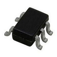
LM94022QBIMG/NOPB National Semiconductor, LM94022QBIMG/NOPB Datasheet - Page 12

LM94022QBIMG/NOPB
Manufacturer Part Number
LM94022QBIMG/NOPB
Description
IC TEMP SENSOR ± 1.5°C TO ± 2.7°C SC70-5
Manufacturer
National Semiconductor
Datasheet
1.LM94022EVAL.pdf
(16 pages)
Specifications of LM94022QBIMG/NOPB
Ic Output Type
Voltage
Sensing Accuracy Range
± 2.7°C
Supply Current
5.4µA
Supply Voltage Range
1.5V To 5.5V
Sensor Case Style
SC-70
No. Of Pins
5
Msl
MSL 1 - Unlimited
Lead Free Status / RoHS Status
Lead free / RoHS Compliant
www.national.com
2.0 Mounting and Thermal
Conductivity
The LM94022 can be applied easily in the same way as other
integrated-circuit temperature sensors. It can be glued or ce-
mented to a surface.
To ensure good thermal conductivity, the backside of the
LM94022 die is directly attached to the GND pin (Pin 2). The
temperatures of the lands and traces to the other leads of the
LM94022 will also affect the temperature reading.
Alternatively, the LM94022 can be mounted inside a sealed-
end metal tube, and can then be dipped into a bath or screwed
into a threaded hole in a tank. As with any IC, the LM94022
and accompanying wiring and circuits must be kept insulated
and dry, to avoid leakage and corrosion. This is especially true
if the circuit may operate at cold temperatures where con-
densation can occur. If moisture creates a short circuit from
the output to ground or V
not be correct. Printed-circuit coatings are often used to en-
sure that moisture cannot corrode the leads or circuit traces.
The thermal resistance junction to ambient (θ
rameter used to calculate the rise of a device junction tem-
perature due to its power dissipation. The equation used to
calculate the rise in the LM94022's die temperature is
where T
rent, I
voltage. For example, in an application where T
V
and I
showing a self-heating error of only 0.021°C. Since the
LM94022's junction temperature is the actual temperature
being measured, care should be taken to minimize the load
current that the LM94022 is required to drive. Figure 1 shows
the thermal resistance of the LM94022.
3.0 Output and Noise
Considerations
A push-pull output gives the LM94022 the ability to sink and
source significant current. This is beneficial when, for exam-
ple, driving dynamic loads like an input stage on an analog-
to-digital converter (ADC). In these applications the source
current is required to quickly charge the input capacitor of the
ADC. See the Applications Circuits section for more discus-
sion of this topic. The LM94022 is ideal for this and other
applications which require strong source or sink current.
The LM94022's supply-noise gain (the ratio of the AC signal
on V
tests. It's typical attenuation is shown in the Typical Perfor-
mance Characteristics section. A load capacitor on the output
can help to filter noise.
For operation in very noisy environments, some bypass ca-
pacitance should be present on the supply within approxi-
mately 2 inches of the LM94022.
DD
Device Number
LM94022BIMG
= 5 V, I
OUT
L
L
= 2 μA, the junction temperature would be 30.021 °C,
is the load current on the output, and V
A
FIGURE 1. LM94022 Thermal Resistance
to the AC signal on V
is the ambient temperature, I
DD
= 9 μA, Gain Select = 11, V
NS Package
DD
MAA05A
Number
, the output from the LM94022 will
DD
) was measured during bench
Q
is the quiescent cur-
Resistance (θ
OUT
415°C/W
Thermal
O
JA
= 2.231 mV,
is the output
) is the pa-
A
= 30 °C,
JA
)
12
4.0 Capacitive Loads
The LM94022 handles capacitive loading well. In an extreme-
ly noisy environment, or when driving a switched sampling
input on an ADC, it may be necessary to add some filtering to
minimize noise coupling. Without any precautions, the
LM94022 can drive a capacitive load less than or equal to
1100 pF as shown in Figure 2. For capacitive loads greater
than 1100 pF, a series resistor may be required on the output,
as shown in Figure 3.
5.0 Output Voltage Shift
The LM94022 is very linear over temperature and supply volt-
age range. Due to the intrinsic behavior of an NMOS/PMOS
rail-to-rail buffer, a slight shift in the output can occur when
the supply voltage is ramped over the operating range of the
device. The location of the shift is determined by the relative
levels of V
V
This slight shift (a few millivolts) takes place over a wide
change (approximately 200 mV) in V
shift takes place over a wide temperature change of 5°C to
20°C, V
in the Electrical Characteristics table already include this pos-
sible shift.
6.0 Selectable Gain for Optimization
and In Situ Testing
The Gain Select digital inputs can be tied to the rails or can
be driven from digital outputs such as microcontroller GPIO
pins. In low-supply voltage applications, the ability to reduce
the gain to -5.5 mV/°C allows the LM94022 to operate over
the full -50 °C to 150 °C range. When a larger supply voltage
FIGURE 3. LM94022 with series resistor for capacitive
OUT
FIGURE 2. LM94022 No Decoupling Required for
= 1.0V.
OUT
Capacitive Loads Less than 1100 pF.
DD
is always monotonic. The accuracy specifications
100 nF to 999 nF
1.1 nF to 99 nF
and V
Loading greater than 1100 pF.
C
1 μF
LOAD
OUT
. The shift typically occurs when V
Minimum R
1.5 kΩ
800 Ω
3 kΩ
DD
or V
S
OUT
. Since the
20143015
20143033
DD
-


