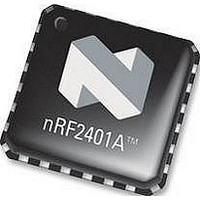
NRF2401GA NORDIC SEMICONDUCTOR, NRF2401GA Datasheet - Page 34

NRF2401GA
Manufacturer Part Number
NRF2401GA
Description
IC, TRANSCEIVER, 2.4GHZ, SMD
Manufacturer
NORDIC SEMICONDUCTOR
Datasheet
1.NRF2401GA.pdf
(39 pages)
Specifications of NRF2401GA
Transmitting Current
13mA
Data Rate
1000Kbps
Frequency Range
2.4GHz To 2.524GHz
Modulation Type
GFSK
Sensitivity Dbm
-90dBm
Rf Ic Case Style
QFN
No. Of Pins
36
Supply Voltage Range
1.9V To 3.6V
Lead Free Status / RoHS Status
Lead free / RoHS Compliant
PRODUCT SPECIFICATION
nRF2401 Single Chip 2.4 GHz Radio Transceiver
frequency. When clocking the nRF2401 externally, XC2 is not used and can be left as
an open pin.
Frequency Reference MCU
In direct mode there is a requirement on the accuracy of the data rate. For the receiver
to detect the incoming data and recover the clock, the data rate must be within
±200ppm, given that the data is "random", i.e. there is a statistical calculation on how
often a preamble like sequence is present in the data. The clock is synchronized for
any preamble detection, be it a dedicated preamble or part of the data stream.
PCB layout and de -coupling guidelines
A well-designed PCB is necessary to achieve good RF performance. Keep in mind
that a poor layout may lead to loss of performance, or even functionality, if due care is
not taken. A fully qualified RF-layout for the nRF2401 and its surrounding
components, including matching networks, can be downloaded from
www.nordicsemi.no.
A PCB with a minimum of two layers including a ground plane is recommended for
optimum performance. The nRF2401 DC supply voltage should be de-coupled as
close as possible to the VDD pins with high performance RF capacitors, see Table 23.
It is preferable to mount a large surface mount capacitor (e.g. 4.7 F tantalum) in
parallel with the smaller value capacitors. The nRF2401 supply voltage should be
filtered and routed separately from the supply voltages of any digital circuitry.
Long power supply lines on the PCB should be avoided. All device grounds, VDD
connections and VDD bypass capacitors must be connected as close as possible to the
nRF2401 IC. For a PCB with a topside RF ground plane, the VSS pins should be
connected directly to the ground plane. For a PCB with a bottom ground plane, the
best technique is to have via holes as close as possible to the VSS pads. One via hole
should be used for each VSS pin.
Full swing digital data or control signals should not be routed close to the crystal or
the power supply lines.
Nordic Semiconductor ASA - Vestre Rosten 81, N-7075 Tiller, Norway -
Phone +4772898900
-
Fax +4772898989
Page 34 of 39
Revision: 1.1
June 2004


