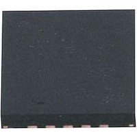
LTC5542IUH#PBF Linear Technology, LTC5542IUH#PBF Datasheet

LTC5542IUH#PBF
Specifications of LTC5542IUH#PBF
Available stocks
Related parts for LTC5542IUH#PBF
LTC5542IUH#PBF Summary of contents
Page 1
... W-CDMA. TD-SCDMA, WiMAX, GSM1800) n Point-to-Point Microwave Links n High Dynamic Range Downmixer Applications L, LT, LTC, LTM, Linear Technology and the Linear logo are registered trademarks of Linear Technology Corporation. All other trademarks are the property of their respective owners. TYPICAL APPLICATION Wideband Receiver 1nF ...
Page 2
... J ORDER INFORMATION LEAD FREE FINISH TAPE AND REEL LTC5542IUH#PBF LTC5542IUH#TRPBF Consult LTC Marketing for parts specifi ed with wider operating temperature ranges. Consult LTC Marketing for information on non-standard lead based fi nish parts. For more information on lead free part marking, go to: For more information on tape and reel specifi ...
Page 3
AC ELECTRICAL CHARACTERISTICS P = –3dBm (Δf = 2MHz for two-tone IIP3 tests),unless otherwise noted. Test circuit shown in Figure 1. (Notes Low-Side LO Downmixer Application 1900 to 2700MHz 190MHz, f PARAMETER ...
Page 4
LTC5542 DC ELECTRICAL CHARACTERISTICS noted. Test circuit shown in Figure 1. (Note 2) PARAMETER Power Supply Requirements ( CCIF V Supply Voltage (Pins 6, 8 and 14 Supply Voltage (Pins 18 and 19) CCIF ...
Page 5
TYPICAL AC PERFORMANCE CHARACTERISTICS V = 3.3V 3.3V, SHDN = Low CCIF 190MHz, unless otherwise noted. Test circuit shown in Figure 1. Conversion Gain, IIP3 and Frequency 28 IIP3 26 ...
Page 6
LTC5542 TYPICAL AC PERFORMANCE CHARACTERISTICS V = 3.3V 3.3V, SHDN = Low CCIF 190MHz, unless otherwise noted. Test circuit shown in Figure 1. 2-Tone IF Output Power, IM3 and IM5 vs RF Input ...
Page 7
TYPICAL AC PERFORMANCE CHARACTERISTICS V = 3.3V 3.3V, SHDN = Low CCIF 190MHz, unless otherwise noted. Test circuit shown in Figure 1. Conversion Gain, IIP3 and Frequency 27 IIP3 25 ...
Page 8
LTC5542 PIN FUNCTIONS NC (Pin 1): This pin is not connected internally. It can be left fl oating, connected to ground (Pin 2): Single-Ended Input for the RF Signal. This pin is internally connected to the ...
Page 9
BLOCK DIAGRAM TEST CIRCUIT 4:1 T1 C10 CCIF 3.1V TO 5.3V 100mA IFBIAS 50Ω C11 LTC5542 GND SHDN 5 ...
Page 10
LTC5542 APPLICATIONS INFORMATION Introduction The LTC5542 consists of a high linearity passive double- balanced mixer core, IF buffer amplifi er, high speed single- pole double-throw (SPDT) LO switch, LO buffer amplifi er and bias/shutdown circuits. See Block Diagram section for ...
Page 11
APPLICATIONS INFORMATION The RF input impedance and input refl ection coeffi cient, versus RF frequency, is listed in Table 1. The reference plane for this data is pin 2 of the IC, with no external matching, and the LO is ...
Page 12
LTC5542 APPLICATIONS INFORMATION The nominal LO input level is 0dBm although the limiting amplifi ers will deliver excellent performance over a ±6dB input power range. LO input power greater than 6dBm may cause conduction of the internal ESD diodes. Series ...
Page 13
APPLICATIONS INFORMATION Bandpass IF Matching The IF output can be matched for IF frequencies as low as 90MHz or as high as 500MHz using the bandpass IF matching shown in Figure 1 and Figure 7. L1 and L2 resonate with ...
Page 14
LTC5542 APPLICATIONS INFORMATION Table 5. Performance Comparison with V (RF = 2400MHz, Low-Side LO 190MHz P1dB CCIF C V (mA) (dB) (dBm) CCIF 3.3V 100 8.0 11.3 5V 103 7.9 14.7 The IFBIAS pin (pin 20) ...
Page 15
... ON THE TOP AND BOTTOM OF PACKAGE Information furnished by Linear Technology Corporation is believed to be accurate and reliable. However, no responsibility is assumed for its use. Linear Technology Corporation makes no representa- tion that the interconnection of its circuits as described herein will not infringe on existing patent rights. UH Package 20-Lead Plastic QFN (5mm × ...
Page 16
... SNR, 78dB SFDR, 740mW Power Consumption www.linear.com ● Wideband Conversion Gain, IIP3 and 27 0 IIP3 1950 ±60MHz 23 – 2040MHz P = 0dBm 3.3V CC CCIF 19 – 25° – RETURN LOSS 11 – – 100110 120130140150 IF OUTPUT FREQUENCY (MHz) 5542 TA03 LT 0310 • PRINTED IN USA © LINEAR TECHNOLOGY CORPORATION 2010 5542f ...


