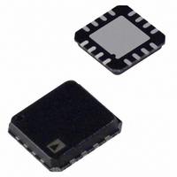
AD8352ACPZ-R7 Analog Devices Inc, AD8352ACPZ-R7 Datasheet - Page 11

AD8352ACPZ-R7
Manufacturer Part Number
AD8352ACPZ-R7
Description
IC, DIFF RF/IF AMP, 25DB 2.2GHZ LFCSP-16
Manufacturer
Analog Devices Inc
Type
Differential Amplifierr
Datasheet
1.AD8352-EVAL.pdf
(20 pages)
Specifications of AD8352ACPZ-R7
Frequency Range
10MHz To 2.5GHz
Power Dissipation Pd
210mW
Supply Current
37mA
Supply Voltage Range
3V To 5.5V
Rf Ic Case Style
LFCSP
No. Of Pins
16
Gain
25dB
Rf Type
General Purpose
Design Resources
Using AD8352 as an Ultralow Distortion Differential RF/IF Front End for High Speed ADCs (CN0046)
Amplifier Type
RF/IF Differential
Number Of Circuits
1
Output Type
Differential
Slew Rate
8000 V/µs
-3db Bandwidth
2.2GHz
Current - Input Bias
75nA
Current - Supply
37mA
Voltage - Supply, Single/dual (±)
3 V ~ 5.5 V
Operating Temperature
-40°C ~ 85°C
Mounting Type
Surface Mount
Package / Case
16-VFQFN, 16-CSP, Exposed Pad
Voltage - Supply
3 V ~ 5 V
Frequency
10MHz ~ 2.5GHz
P1db
15.5dBm
Test Frequency
140MHz
Number Of Channels
1
Number Of Elements
1
Power Supply Requirement
Single
Common Mode Rejection Ratio
57dB
Single Supply Voltage (typ)
5V
Dual Supply Voltage (typ)
Not RequiredV
Power Dissipation
210mW
Rail/rail I/o Type
No
Single Supply Voltage (min)
3V
Single Supply Voltage (max)
5.5V
Dual Supply Voltage (min)
Not RequiredV
Dual Supply Voltage (max)
Not RequiredV
Operating Temp Range
-40C to 85C
Operating Temperature Classification
Industrial
Mounting
Surface Mount
Pin Count
16
Package Type
LFCSP EP
Rohs Compliant
Yes
Lead Free Status / RoHS Status
Lead free / RoHS Compliant
Noise Figure
-
Lead Free Status / Rohs Status
Compliant
Other names
AD8352ACPZ-R7
APPLICATIONS INFORMATION
GAIN AND DISTORTION ADJUSTMENT
(DIFFERENTIAL INPUT)
Table 5 and Table 6 show the required value of R
specified at 200 Ω and 1 kΩ loads. Figure 22 and Figure 24 plot
gain vs. R
loads (R
where
R
R
The third-order harmonic distortion can be reduced by using
external components R
required values for R
(single tone) third-order distortion reduction at 180 MHz.
Figure 23 and Figure 25 show any gain (up to 18 dB) vs. C
200 Ω and 1 kΩ loads, respectively. When these values are selected,
they result in minimum single tone, third-order distortion at
180 MHz. This frequency point provides the best overall broad-
band distortion for the specified frequencies below and above
this value. For applications above ~300 MHz, C
not required. See the Specifications section and the third-order
harmonic plots for more details (see Figure 12, Figure 14, and
Figure 15).
C
below 180 MHz that result in relatively lower third-order (in-
band) intermodulation distortion terms. See the Narrow-Band,
Third-Order Intermodulation Cancellation section for more
information. Though not shown, single tone, third-order
optimization can also be improved for narrow-band frequency
applications below 180 MHz with the proper selection of C
and 3 dB to 6 dB of relative third-order improvement can be
realized at frequencies below approximately 140 MHz.
Using the information listed in Table 5 and Table 6, an extrapolated
value for R
For loads above 1 kΩ, use the 1 kΩ R
Table 5. Broadband Selection of RG, CD, and RD, 200 Ω Load
A
3
6
9
10
12
15
18
L
G
D
V
is the single-ended load.
is the gain setting resistor.
(dB)
can be further optimized for narrow-band tuning requirements
A
V
L
Differenti
), use Equation 1 to compute gain vs. R
G
up to 18 dB for both load conditions. For other output
D
can be determined for loads between 200 Ω and 1 kΩ.
al
=
R
390
220
140
115
86
56
35
⎛
⎜
⎜
⎝
G
(
(Ω)
R
D
G
and C
+
D
5)
and C
R
(
G
R
D
+
L
for the specified gains to achieve
D
+
500
. Table 5 and Table 6 show the
53)
C
Open
Open
0.1
0.2
0.3
0.6
1
D
+
(pF)
D
430
values listed in Table 6.
⎞
⎟
⎟
⎠
R
L
D
G
G
and R
.
for the gains
R
6.8
4.3
4.3
4.3
4.3
4.3
4.3
D
(kΩ)
D
are
D
D
for
,
Rev. B | Page 11 of 20
(1)
Table 6. Broadband Selection of R
A
3
6
9
10
12
15
18
V
(dB)
20
18
16
14
12
10
20
18
16
14
12
10
8
6
4
2
0
8
6
4
2
0
0
0
0.1
50
R
750
360
210
180
130
82
54
G
Figure 22. Gain vs. R
0.2
Figure 23. Gain vs. C
(Ω)
100
0.3
150
0.4
C
R
D
200
G
0.5
C
Open
Open
Open
0.05
0.1
0.3
0.5
(pF)
(Ω)
D
G
D
G
, R
, R
(pF)
, C
0.6
L
L
250
= 200 Ω
= 200 Ω
D
, and R
0.7
300
0.8
D
, 1 kΩ Load
R
6.8
6.8
6.8
6.8
6.8
6.8
6.8
350
D
AD8352
0.9
(kΩ)
400
1.0


