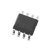
SC1101CS.TRT Semtech, SC1101CS.TRT Datasheet - Page 4

SC1101CS.TRT
Manufacturer Part Number
SC1101CS.TRT
Description
IC, VOLTAGE MODE PWM CTRL, 5.25V, 8-SOIC
Manufacturer
Semtech
Datasheet
1.SC1101CS.TR.pdf
(7 pages)
Specifications of SC1101CS.TRT
Input Voltage
7V
Output Current
500mA
Frequency
230kHz
Supply Voltage Range
4.75V To 5.25V
Digital Ic Case Style
SOIC
No. Of Pins
8
Operating Temperature Range
0°C To +70°C
Lead Free Status / RoHS Status
Lead free / RoHS Compliant
Applications Information
Layout Guidelines
Careful attention to layout requirements are necessary
for successful implementation of the SC1101 PWM
controller. High currents switching at 200kHz are present
in the application and their effect on ground plane volt-
age differentials must be understood and minimized.
1). The high power parts of the circuit should be laid out
first. A ground plane should be used, the number and
position of ground plane interruptions should be such as
to not unnecessarily compromise ground plane integrity.
Isolated or semi-isolated areas of the ground plane may
be deliberately introduced to constrain ground currents
to particular areas, for example the input capacitor and
bottom Schottky ground.
2). The loop formed by the Input Capacitor(s) (Cin), the
Top FET (Q1) and the Schottky (D1) must be kept as small
as possible. This loop contains all the high current, fast
transition switching. Connections should be as wide and
as short as possible to minimize loop inductance. Mini-
mizing this loop area will reduce EMI, lower ground injec-
tion currents, resulting in electrically “cleaner” grounds
for the rest of the system and minimize source ringing,
resulting in more reliable gate switching signals.
3). The connection between the junction of Q1, D1 and
the output inductor should be a wide trace or copper
region. It should be as short as practical. Since this con-
nection has fast voltage transitions, keeping this con-
nection short will minimize EMI. The connection between
the output inductor and the sense resistor should be a
wide trace or copper area, there are no fast voltage or
current transitions in this connection and length is not
so important, however adding unnecessary impedance
will reduce efficiency.
4) The Output Capacitor(s) (Cout) should be located as
close to the load as possible, fast transient load cur-
POWER MANAGEMENT
2005 Semtech Corp.
4
rents are supplied by Cout only, and connections between
Cout and the load must be short, wide copper areas to
minimize inductance and resistance.
5) The SC1101 is best placed over an isolated ground
plane area. GND and PGND should be returned to this
isolated ground. This isolated ground area should be con-
nected to the main ground by a trace that runs from the
GND pin to the ground side of (one of) the output
capacitor(s). If this is not possible, the GND pin may be
connected to the ground path between the Output
Capacitor(s) and the Cin, Q1, D1 loop. Under no circum-
stances should GND be returned to a ground inside the
Cin, Q1, D1 loop.
6) Vcc for the SC1101 should be supplied from the 5V
supply through a 10
decoupled directly to GND by a 0.1µF ceramic capacitor,
trace lengths should be as short as possible.
7) The Current Sense resistor and the divider across it
should form as small a loop as possible, the traces run-
ning back to CS(+) and CS(-) on the SC1101 should run
parallel and close to each other.
8) To minimize noise pickup at the sensitive FB pin, the
feedback resistors should both be close to the SC1101
with the bottom resistor (Rb) returned to ground at the
GND pin.
Under Voltage Lockout
The under voltage lockout circuit of the SC1101 assures
that the high-side MOSFET driver outputs remain in the
off state whenever the supply voltage drops below set
parameters. Lockout occurs if V
mal operation resumes once V
resistor, the Vcc pin should be
CC
CC
rises above 3.8V.
falls below 3.8V. Nor-
www.semtech.com
SC1101


