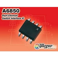
A6850KL-T Allegro Microsystems Inc, A6850KL-T Datasheet - Page 6

A6850KL-T
Manufacturer Part Number
A6850KL-T
Description
IC, 2CH SWITCH INTERFACE, 26.5V, 8-SOIC
Manufacturer
Allegro Microsystems Inc
Datasheet
1.A6850KLTR-T.pdf
(12 pages)
Specifications of A6850KL-T
Power Load Switch Type
Low Side
Input Voltage
26.5V
On State Resistance
35ohm
Thermal Protection
Yes
On / Enable Input Polarity
Active High
No. Of Outputs
2
Current Limit
35mA
Lead Free Status / RoHS Status
Lead free / RoHS Compliant
A6850
Signal and Enable delays
When ENABLEx = 1, current signals applied to the OUTPUTx
pins will appear scaled and delayed on the SENSEx pins. The
transfer characteristic can be considered that of a low pass filter.
The response time definitions are given in figures 1 and 2, in the
Characteristic Performance section.
The rise time response is dependent on the effective capacitance
loading on the SENSEx pin.
The RC time constant, , can be estimated using:
where R
be in ns.
The 10% to 90% rise time, t
The small signal low pass filter bandwidth based on a single pole
response may be estimated using:
The result is in MHz when t
If the values of t
ter estimate may be given by:
The result is in MHz when t
Each signal channel may be enabled or disabled individually via
their respective ENABLEx pins, as shown in table 1.
Table 1. Enable/Disable Signal Channel Truth Table
*Sleep mode
EN1
L*
H
H
BW= 350 / t
BW= 700 / (t
L
t
rLH
= R
SENSEx
= 2.2 ×
SENSEx
EN2
L*
is in kΩ and C
H
H
L
rLH
rLH
rLH
and t
(90 + C
+ t
IOU1
fHL
fHL
I
I
0
0
1
1
rLH
rLH
SENSE
rLH
are significantly different then a bet-
)
SENSE
, may be estimated from:
is in ns.
and t
)
IOU2
is in pF; the result will
fHL
I
I
0
0
2
2
are in ns.
SEN1
I
I
1
1
/ 10
/ 10
0
0
SEN2
(2)
(3)
(4)
(5)
I
I
2
2
/ 10
/ 10
0
0
Dual Channel Switch Interface IC
When a capacitor is added in parallel with the signal source con-
nected to an OUTPUTx pin, additional allowance must be made
for settling time caused by the inrush current needed to recharge a
partially, or fully discharged, capacitor which has decayed during
the disabled period.
During this time the current required may reach I
current limit value for the OUTPUTx pins.
The effects will be most noticeable on a SENSEx pin and will
usually cause a signal overshoot as shown as t
Thermal Shutdown (TSD)
The A6850 protects itself from excessive heat damage by
disabling both outputs when the junction temperature, T
above the TSD threshold (T
until the junction temperature falls below the T
the TSD hysteresis, T
Figure 4. Overshoot resulting from additional capacitance.
OUTPUTx
ENABLEx
SENSEx
0 mA
0 V
TSDhys
115 Northeast Cutoff
1.508.853.5000; www.allegromicro.com
Allegro MicroSystems, Inc.
Worcester, Massachusetts 01615-0036 U.S.A.
.
TSD
). The outputs will remain off
50%
t
ENdlyLH
ENsettle
TSD
OUTPUTM
level minus
in figure 4.
t
ENsettle
J
, rises
, the
6


