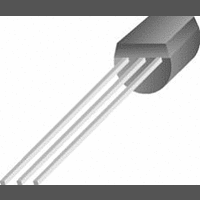
LM317LZ National Semiconductor, LM317LZ Datasheet - Page 6

LM317LZ
Manufacturer Part Number
LM317LZ
Description
IC, ADJ LINEAR REG, 1.2V TO 37V, TO-92-3
Manufacturer
National Semiconductor
Datasheet
1.LM317LITPNOPB.pdf
(20 pages)
Specifications of LM317LZ
Primary Input Voltage
40V
Output Voltage Adjustable Range
1.2V To 37V
Dropout Voltage Vdo
1.8V
No. Of Outputs
1
No. Of Pins
3
Output Current
100mA
Lead Free Status / RoHS Status
Contains lead / RoHS non-compliant
Available stocks
Company
Part Number
Manufacturer
Quantity
Price
Company:
Part Number:
LM317LZ
Manufacturer:
FSC
Quantity:
90 000
Company:
Part Number:
LM317LZ
Manufacturer:
ST/FSC
Quantity:
22 000
Part Number:
LM317LZ
Manufacturer:
TI/德州仪器
Quantity:
20 000
Company:
Part Number:
LM317LZ/NOPB
Manufacturer:
TOREX
Quantity:
12 000
Part Number:
LM317LZ/NOPB
Manufacturer:
NS/国半
Quantity:
20 000
Company:
Part Number:
LM317LZG
Manufacturer:
ON Semiconductor
Quantity:
37 788
Part Number:
LM317LZG
Manufacturer:
ON/安森美
Quantity:
20 000
www.national.com
Application Hints
In operation, the LM317L develops a nominal 1.25V reference
voltage, V
The reference voltage is impressed across program resistor
R1 and, since the voltage is constant, a constant current I
then flows through the output set resistor R2, giving an output
voltage of
Since the 100μA current from the adjustment terminal repre-
sents an error term, the LM317L was designed to minimize
I
do this, all quiescent operating current is returned to the out-
put establishing a minimum load current requirement. If there
is insufficient load on the output, the output will rise.
EXTERNAL CAPACITORS
An input bypass capacitor is recommended in case the reg-
ulator is more than 6 inches away from the usual large filter
capacitor. A 0.1μF disc or 1μF solid tantalum on the input is
suitable input bypassing for almost all applications. The de-
vice is more sensitive to the absence of input bypassing when
adjustment or output capacitors are used, but the above val-
ues will eliminate the possibility of problems.
The adjustment terminal can be bypassed to ground on the
LM317L to improve ripple rejection and noise. This bypass
capacitor prevents ripple and noise from being amplified as
the output voltage is increased. With a 10μF bypass capacitor
80dB ripple rejection is obtainable at any output level. In-
creases over 10μF do not appreciably improve the ripple
rejection at frequencies above 120Hz. If the bypass capacitor
is used, it is sometimes necessary to include protection
diodes to prevent the capacitor from discharging through in-
ternal low current paths and damaging the device.
In general, the best type of capacitors to use is solid tantalum.
Solid tantalum capacitors have low impedance even at high
frequencies. Depending upon capacitor construction, it takes
about 25μF in aluminum electrolytic to equal 1μF solid tanta-
lum at high frequencies. Ceramic capacitors are also good at
high frequencies; but some types have a large decrease in
capacitance at frequencies around 0.5MHz. For this reason,
a 0.01μF disc may seem to work better than a 0.1μF disc as
a bypass.
ADJ
and make it very constant with line and load changes. To
REF
, between the output and adjustment terminal.
FIGURE 1.
906407
1
6
Although the LM317L is stable with no output capacitors, like
any feedback circuit, certain values of external capacitance
can cause excessive ringing. This occurs with values be-
tween 500pF and 5000pF. A 1μF solid tantalum (or 25μF
aluminum electrolytic) on the output swamps this effect and
insures stability.
LOAD REGULATION
The LM317L is capable of providing extremely good load reg-
ulation but a few precautions are needed to obtain maximum
performance. The current set resistor connected between the
adjustment terminal and the output terminal (usually 240Ω)
should be tied directly to the output of the regulator rather than
near the load. This eliminates line drops from appearing ef-
fectively in series with the reference and degrading regula-
tion. For example, a 15V regulator with 0.05Ω resistance
between the regulator and load will have a load regulation due
to line resistance of 0.05Ω × I
near the load the effective line resistance will be 0.05Ω (1 +
R2/R1) or in this case, 11.5 times worse.
Figure 2
and 240Ω set resistor.
With the TO-92 package, it is easy to minimize the resistance
from the case to the set resistor, by using two separate leads
to the output pin. The ground of R2 can be returned near the
ground of the load to provide remote ground sensing and im-
prove load regulation.
THERMAL REGULATION
When power is dissipated in an IC, a temperature gradient
occurs across the IC chip affecting the individual IC circuit
components. With an IC regulator, this gradient can be espe-
cially severe since power dissipation is large. Thermal regu-
lation is the effect of these temperature gradients on output
voltage (in percentage output change) per watt of power
change in a specified time. Thermal regulation error is inde-
pendent of electrical regulation or temperature coefficient,
and occurs within 5ms to 50ms after a change in power dis-
sipation. Thermal regulation depends on IC layout as well as
electrical design. The thermal regulation of a voltage regulator
is defined as the percentage change of V
the first 10ms after a step of power is applied. The LM317L
specification is 0.2%/W, maximum.
In the Thermal Regulation curve at the bottom of the Typical
Performance Characteristics page, a typical LM317L's output
changes only 7mV (or 0.07% of V
pulse is applied for 10ms. This performance is thus well inside
the specification limit of 0.2%/W × 1W = 0.2% maximum.
When the 1W pulse is ended, the thermal regulation again
shows a 7mV change as the gradients across the LM317L
FIGURE 2. Regulator with Line Resistance
shows the effect of resistance between the regulator
in Output Lead
L
. If the set resistor is connected
OUT
= −10V) when a 1W
OUT
, per watt, within
906408


