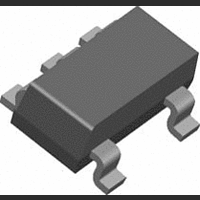
SP6201EM5-L-ADJ Exar Corporation, SP6201EM5-L-ADJ Datasheet - Page 3

SP6201EM5-L-ADJ
Manufacturer Part Number
SP6201EM5-L-ADJ
Description
IC, ADJ LDO REG 2.7V TO 6V 0.2A 5-SOT-23
Manufacturer
Exar Corporation
Datasheet
1.SP6201EM5-L-2-5.pdf
(17 pages)
Specifications of SP6201EM5-L-ADJ
Primary Input Voltage
6V
Output Voltage Adjustable Range
2.7V To 6V
Dropout Voltage Vdo
160mV
No. Of Pins
5
Output Current
200mA
Operating Temperature Range
-40°C To +125°C
Lead Free Status / RoHS Status
Lead free / RoHS Compliant
Available stocks
Company
Part Number
Manufacturer
Quantity
Price
Company:
Part Number:
SP6201EM5-L-ADJ
Manufacturer:
SIPEX
Quantity:
2 000
Part Number:
SP6201EM5-L-ADJ
Manufacturer:
SIPEX
Quantity:
20 000
V
specifications which apply over the full operating temperature range, unless otherwise specified.
Note 1. Exceeding the absolute maximum rating may damage the device.
Note 2. The device is not guaranteed to function outside its operating rating.
Note 3. The maximum allowable power dissipation at any T
Exceeding the maximum allowable power dissipation will result in excessive die temperature, and the regulator will
go into thermal shutdown. The θ
the DFN package on a standard 4 layer board (see “Thermal Considerations” section for further details).
Note 4. Output voltage temperature coefficient is defined as the worst case voltage change divided by the total
temperature range.
Note 5. Load Regulation is measured at constant junction temperature using low duty cycle pulse testing. Parts are
tested for load regulation in the load range; from 0.1mA to 100mA, SP6200; from 0.1mA to 200mA, SP6201. Changes
in output voltage due to heating effects are covered by the thermal regulation specification. Not applicable to output
voltages less than 2.5V.
Note 6. Dropout Voltage is defined as the input to output differential at which the output voltage drops 2% below
its nominal value measured at 1V differential. Not applicable to output voltages less than 2.7V.
Note 7. Ground pin current is the regulator quiescent current. The total current drawn from the supply is the sum
of the load current plus the ground pin current.
Note 8. Thermal regulation is defined as the change in output voltage at a time ”t” after a change in power dissipation
is applied, excluding load or line regulation effects. Specifications are for a 100mA load pulse at V
Date: 5/5/06 Rev A
PARAMETER
Thermal Regulation,
Note 8, (∆V
Output Noise, (e
ENABLE INPUT
Enable Input Logic-Low Voltage,
(V
Enable Input Logic-High Voltage,
(V
Enable Input Current, (I
Reset Not Output
IN
= V
IL
IH
)
)
OUT
+1V, V
O
/∆P
O
= 5V for ADJ, I
D
no
)
)
IL
), (I
L
IH
= 100µA, C
)
JA
of the SP6200/6201 (all versions) is 191°C/W for the SOT-23-5 and 59°C/W for
IN
= 1.0µF, C
MIN
1.6
-2
SP6200/6201 100/200mA CMOS LDO Regulator
OUT
TYP
0.05
0.01
0.01
150
-4
= 1.0µF, T
ELECTRICAL CHARACTERISTICS: Continued
MAX
0.4
-6
1
1
3
J
= 25
A
°
(ambient temperature) is P
C , unless otherwise specified. The ♦ denotes the
UNITS
µVrms
%/W
µA
µA
%
V
V
♦ ♦ ♦ ♦ ♦
♦
♦
♦
♦
CONDITIONS
I
0.1µF from V
10Hz to 100kHz
Regulator Shutdown
Regulator Enabled
V
V
Threshold
L
IL
IH
= 50mA, C
< 0.4V
> 2.0V
© Copyright 2006 Sipex Corporation
D (MAX)
L
OUT
= 1µF
= (T
IN
to Adj.
= 6V for t = 10ms.
J (MAX)
– T
A
) / θ
ϑA
.


