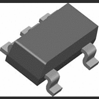
LP2981IM5-2.5 National Semiconductor, LP2981IM5-2.5 Datasheet - Page 13

LP2981IM5-2.5
Manufacturer Part Number
LP2981IM5-2.5
Description
IC, LDO VOLT REG, 2.5V, 0.1A, 5-SOT-23
Manufacturer
National Semiconductor
Datasheet
1.LP2981IM5X-3.3.pdf
(16 pages)
Specifications of LP2981IM5-2.5
Primary Input Voltage
16V
Output Voltage Fixed
2.5V
Dropout Voltage Vdo
200mV
No. Of Pins
5
Output Current
100mA
Operating Temperature Range
-40°C To +125°C
Termination Type
SMD
Lead Free Status / RoHS Status
Contains lead / RoHS non-compliant
Available stocks
Company
Part Number
Manufacturer
Quantity
Price
Company:
Part Number:
LP2981IM5-2.5
Manufacturer:
NS
Quantity:
1 000
Part Number:
LP2981IM5-2.5
Manufacturer:
NS/国半
Quantity:
20 000
REVERSE CURRENT PATH
The internal PNP power transistor used as the pass element
in the LP2981 has an inherent diode connected between the
regulator output and input. During normal operation (where
the input voltage is higher than the output) this diode is re-
verse biased (See Figure 5).
However, if the input voltage is more than a V
output voltage, this diode will turn ON and current will flow into
the regulator output. In such cases, a parasitic SCR can latch
which will allow a high current to flow into the V
the ground pin, which can damage the part.
The internal diode can also be turned on if the input voltage
is abruptly stepped down to a voltage which is a V
the output voltage.
FIGURE 5. LP2981 Reverse Current Path
FIGURE 4. 3V/10 μF ESR Curves
1250642
IN
BE
1250641
pin and out
below the
BE
below
13
In any application where the output voltage may be higher
than the input voltage, an external Schottky diode must be
connected from V
V
LP2981 to 0.3V (see Absolute Maximum Ratings)
ON/OFF INPUT OPERATION
The LP2981 is shut off by pulling the ON/OFF input low, and
turned on by driving the input high. If this feature is not to be
used, the ON/OFF input should be tied to V
ulator on at all times (the ON/OFF input must not be left
floating).
To ensure proper operation, the signal source used to drive
the ON/OFF input must be able to swing above and below the
specified turn-on/turn-off voltage thresholds which guarantee
an ON or OFF state (see Electrical Characteristics).
The ON/OFF signal may come from either a totem-pole out-
put, or an open-collector output with pull-up resistor to the
LP2981 input voltage or another logic supply. The high-level
voltage may exceed the LP2981 input voltage, but must re-
main within the Absolute Maximum Ratings for the ON/OFF
pin.
It is also important that the turn-on/turn-off voltage signals
applied to the ON/OFF input have a slew rate which is greater
than 40 mV/μs.
IMPORTANT: The regulator shutdown function will not oper-
ate correctly if a slow-moving signal is applied to the ON/OFF
input.
FIGURE 6. Adding External Schottky Diode Protection
OUT
. See Figure 6), to limit the reverse voltage across the
IN
to V
OUT
(cathode on V
IN
to keep the reg-
IN
, anode on
www.national.com
1250643


