LP2950ACZ-5.0 National Semiconductor, LP2950ACZ-5.0 Datasheet - Page 15
LP2950ACZ-5.0
Manufacturer Part Number
LP2950ACZ-5.0
Description
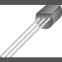
IC, LDO VOLT REG, 5.1V, 0.1A, TO-92-3
Manufacturer
National Semiconductor
Datasheet
1.LP2951CMXNOPB.pdf
(26 pages)
Specifications of LP2950ACZ-5.0
Primary Input Voltage
30V
Output Voltage Fixed
5.1V
Dropout Voltage Vdo
380mV
No. Of Pins
3
Output Current
100mA
Operating Temperature Range
-40°C To +125°C
Termination Type
Through Hole
Lead Free Status / RoHS Status
Contains lead / RoHS non-compliant
Available stocks
Company
Part Number
Manufacturer
Quantity
Price
Company:

Part Number:
LP2950ACZ-5.0
Manufacturer:
ON
Quantity:
18
Part Number:
LP2950ACZ-5.0
Manufacturer:
NS/国半
Quantity:
20 000
Company:
Part Number:
LP2950ACZ-5.0RAG
Manufacturer:
ON Semiconductor
Quantity:
4 600
Part Number:
LP2950ACZ-5.0RAG
Manufacturer:
ON/安森美
Quantity:
20 000


*See Application Hints
**Drive with TTL-high to shut down. Ground or leave open if shutdown fea-
ture is not to be used.
Note: Pins 2 and 6 are left open.
REDUCING OUTPUT NOISE
In reference applications it may be advantageous to reduce
the AC noise present at the output. One method is to reduce
the regulator bandwidth by increasing the size of the output
capacitor. This is the only way noise can be reduced on the
3 lead LP2950 but is relatively inefficient, as increasing the
capacitor from 1μF to 220μF only decreases the noise from
430μV to 160μV rms for a 100kHz bandwidth at 5V output.
Noise can be reduced fourfold by a bypass capacitor across
R
Pick
or about 0.01μF. When doing this, the output capacitor must
be increased to 3.3μF to maintain stability. These changes
reduce the output noise from 430μV to 100μV rms for a
1
, since it reduces the high frequency gain from 4 to unity.
FIGURE 2. Adjustable Regulator
854607
15
100kHz bandwidth at 5V output. With the bypass capacitor
added, noise no longer scales with output voltage so that im-
provements are more dramatic at higher output voltages.
LLP MOUNTING
The SDC08A (No Pullback) 8-Lead LLP package requires
specific mounting techniques which are detailed in National
Semiconductor Application Note # 1187. Referring to the sec-
tion PCB Design Recommendations in AN-1187 (Page 5),
it should be noted that the pad style which should be used
with the LLP package is the NSMD (non-solder mask defined)
type. Additionally, it is recommended the PCB terminal pads
to be 0.2 mm longer than the package pads to create a solder
fillet to improve reliability and inspection.
The thermal dissipation of the LLP package is directly related
to the printed circuit board construction and the amount of
additional copper area connected to the DAP.
The DAP (exposed pad) on the bottom of the LLP package is
connected to the die substrate with a conductive die attach
adhesive. The DAP has no direct electrical (wire) connection
to any of the eight pins. There is a parasitic PN junction be-
tween the die substrate and the device ground. As such, it is
strongly recommend that the DAP be connected directly to
the ground at device lead 4 (i.e. GND). Alternately, but not
recommended, the DAP may be left floating (i.e. no electrical
connection). The DAP must not be connected to any potential
other than ground.
For the LP2951 in the SDC08A 8-Lead LLP package, the
junction-to-case thermal rating, θ
case is the bottom of the package at the center of the DAP.
The junction-to-ambient thermal performance for the LP2951
in the SDC08A 8-Lead LLP package, using the JEDEC
JESD51 standards is summarized in the following table:
JESD 51-3
JESD 51-7
2-Layer
4-Layer
JEDEC
JEDEC
Board
Type
Thermal
None
Vias
1
2
4
6
JC
14.2°C/W
14.2°C/W
14.2°C/W
14.2°C/W
14.2°C/W
, is 14.2°C/W, where the
θ
JC
www.national.com
185°C/W
68°C/W
60°C/W
51°C/W
48°C/W
θ
JA
Related parts for LP2950ACZ-5.0
Image
Part Number
Description
Manufacturer
Datasheet
Request
R

Part Number:
Description:
National Semiconductor [8-Bit D/A Converter]
Manufacturer:
National Semiconductor
Datasheet:
Part Number:
Description:
National Semiconductor [Media Coprocessor]
Manufacturer:
National Semiconductor
Datasheet:
Part Number:
Description:
Digitally Controlled Tone and Volume Circuit with Stereo Audio Power Amplifier, Microphone Preamp Stage and National 3D Sound
Manufacturer:
National Semiconductor
Datasheet:
Part Number:
Description:
Digitally Controlled Tone and Volume Circuit with Stereo Audio Power Amplifier, Microphone Preamp Stage and National 3D Sound
Manufacturer:
National Semiconductor
Datasheet:
Part Number:
Description:
AC97 Rev 2 Codec with Sample Rate Conversion and National 3D Sound
Manufacturer:
National Semiconductor
Part Number:
Description:
Manufacturer:
National Semiconductor
Datasheet:
Part Number:
Description:
Manufacturer:
National Semiconductor
Datasheet:
Part Number:
Description:
General Purpose, Low Voltage, Low Power, Rail-to-Rail Output Operational Amplifiers
Manufacturer:
National Semiconductor
Datasheet:
Part Number:
Description:
8-bit 20 MSPS flash A/D converter.
Manufacturer:
National Semiconductor
Datasheet:
Part Number:
Description:
Low Noise Quad Operational Amplifier
Manufacturer:
National Semiconductor
Datasheet:
Part Number:
Description:
Quad Differential Line Receivers
Manufacturer:
National Semiconductor
Datasheet:
Part Number:
Description:
Quad High Speed Trapezoidal? Bus Transceiver
Manufacturer:
National Semiconductor
Datasheet:
Part Number:
Description:
Dual Line Receiver
Manufacturer:
National Semiconductor
Datasheet:
Part Number:
Description:
TTL to 10k ECL Level Translator with Latch
Manufacturer:
National Semiconductor
Datasheet: