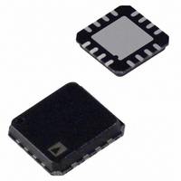
ADP1755ACPZ-R7 Analog Devices Inc, ADP1755ACPZ-R7 Datasheet - Page 13

ADP1755ACPZ-R7
Manufacturer Part Number
ADP1755ACPZ-R7
Description
IC ADJ LDO REG 0.75V TO 3V 1.2A LFCSP-16
Manufacturer
Analog Devices Inc
Datasheet
1.ADP1754-BL1-EVZ.pdf
(20 pages)
Specifications of ADP1755ACPZ-R7
Primary Input Voltage
3.6V
Output Voltage Adjustable Range
0.75V To 3V
Dropout Voltage Vdo
200mV
No. Of Pins
16
Output Current
1.2A
Operating Temperature Range
-40°C To +125°C
Package / Case
16-LFCSP
Mounting Type
Surface Mount
Current - Output
1.2A (Max)
Voltage - Output
0.75 ~ 3 V
Voltage - Input
1.6 ~ 3.6 V
Operating Temperature
-40°C ~ 125°C
Regulator Topology
Positive Adjustable
Voltage - Dropout (typical)
0.105V @ 1.2A
Number Of Regulators
1
Current - Limit (min)
1.5A
Lead Free Status / RoHS Status
Lead free / RoHS Compliant
Available stocks
Company
Part Number
Manufacturer
Quantity
Price
Company:
Part Number:
ADP1755ACPZ-R7
Manufacturer:
ATMEL
Quantity:
101
Part Number:
ADP1755ACPZ-R7
Manufacturer:
ADI/亚德诺
Quantity:
20 000
Figure 31. Typical PG Behavior vs. V
1
2 2
1
2 2
Figure 30. Typical PG Behavior vs. V
CH1
CH3
CH1
CH3
V
C
OUT
IN
1V/DIV
1V/DIV
1.0V
1.0V
1.0V
1.0V
V
V
= C
IN
IN
= 1.5V
OUT
B
B
B
B
W
W
W
W
= 4.7µF
CH2 500mV
CH2 500mV
500mV/DIV
V
OUT
B
B
T
T
W
W
500mV/DIV
M40.0µs
M40.0µs
V
T
T
OUT
OUT
OUT
1V/DIV
1V/DIV
50.40%
50.40%
, V
PG
PG
, V
IN
IN
V
C
Falling (V
Rising (V
OUT
IN
A CH3
A CH3
= C
= 1.5V
OUT
OUT
OUT
= 4.7µF
900mV
900mV
= 1.5 V)
= 1.5 V)
Rev. B | Page 13 of 20
REVERSE CURRENT PROTECTION FEATURE
The ADP1754/ADP1755 have additional circuitry to protect
against reverse current flow from VOUT to VIN. For a typical
LDO with a PMOS pass device, there is an intrinsic body diode
between VIN and VOUT. When V
diode is reverse-biased. If V
diode becomes forward-biased and conducts current from VOUT
to VIN, potentially causing destructive power dissipation. The
reverse current protection circuitry detects when V
than V
tion, reverse-biasing the diode. The gate of the PMOS pass
device is also connected to VOUT, keeping the device off.
Figure 32 shows a plot of the reverse current vs. the V
differential.
4000
3500
3000
2500
2000
1500
1000
500
0
IN
0
and reverses the direction of the intrinsic diode connec-
0.3
0.6
Figure 32. Reverse Current vs. V
0.9
1.2
V
1.5
OUT
OUT
1.8
– V
is greater than V
IN
2.1
ADP1754/ADP1755
(V)
IN
is greater than V
2.4
2.7
OUT
− V
3.0
IN
IN
OUT
3.3
, the intrinsic
is greater
OUT
3.6
OUT
, this
to V
IN


