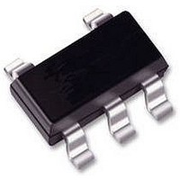
XC6219B182MR Torex Semiconductor Ltd, XC6219B182MR Datasheet

XC6219B182MR
Specifications of XC6219B182MR
Available stocks
Related parts for XC6219B182MR
XC6219B182MR Summary of contents
Page 1
XC6219 Series Preliminary : 25 µA (TYP) Low Power Consumption Output Current : 150 mA (VOUT < 1.7V) Dropout Voltage : 60mV (IOUT=30mA) Output Current : More than 150 mA (300mA limit) : ±2% (±30mV when VOUT=1.5V) Highly Accurate Output ...
Page 2
XC6219 Series Preliminary Pin Configuration VIN VOUT VSS (NC) V OUT VSS SOT-25 SOT-89 (SOT-23-5) [TOP VIEW] [TOP VIEW] Block Diagram CE ON/OFF Control ...
Page 3
XC6219 Series Preliminary Product Classification Selection Guide The following options for the CE pin logic and internal pull-up/down are available: Active 'High pull-down resistor built-in (standard) Active 'High' + 2.0MΩ pull-down resistor built-in <between CE-VSS> (semi-custom) Active 'Low' ...
Page 4
XC6219 Series Preliminary Electrical Characteristics PARAMETER Output Voltage Maximum Output Current Load Regulation Dropout Voltage Supply Current Standby Current Line Regulation ∆V Input Voltage Output Voltage ∆Topr ⋅ V Temperature Characteristics Ripple Rejection Rate Current Limiter Short-circuit Current EN "High" ...
Page 5
XC6219 Series Preliminary Test Circuits 1 Circuit CIN=1.0µF (ceramic Circuit A 3 Circuit 4 Circuit VIN={VOUT+1}V DC +0.5V p-pAC High Speed LDO Regulator VIN VOUT CE VSS V VIN VOUT CE A VSS VIN VOUT CIN=1.0µF (ceramic) CE ...
Page 6
XC6219 Series Preliminary Operational Explanation Output voltage control with the XC6219 series: The voltage divided by resistors R1 & compared with the internal reference voltage by the error amplifier. The P-Channel MOSFET, which is connected to the VOUT ...
Page 7
XC6219 Series Preliminary Typical Performance Characteristics (1) Output Voltage vs. Output Current XC6219x182 CIN=1uF (ceramics), CL=1uF (ceramics) 2.0 1.5 1.0 0.5 0 100 150 200 250 300 350 400 Output Current IOUT (mA) XC6219x252 CIN=1uF (ceramics), CL=1uF (ceramics) ...
Page 8
XC6219 Series Preliminary (2) Output Voltage vs. Input Voltage XC6219x182 CIN=1uF (ceramics), CL=1uF (ceramics) 2.0 1.8 1.6 1.4 1.2 1.0 1.3 1.8 Input Voltage VIN (V) XC6219x252 CIN=1uF (ceramics), CL=1uF (ceramics) 2.7 2.5 2.3 2.1 1.9 1.7 2 2.5 Input ...
Page 9
XC6219 Series Preliminary (3) Input Voltage vs. Output Current XC6219x182 CIN=1uF (ceramics), CL=1uF (ceramics) 1.0 0.8 Topr 0 0.4 0.2 0 120 Output Current IOUT (mA) XC6219x302 ...
Page 10
XC6219 Series Preliminary (4) Supply Current vs. Input Voltage (Continued) XC6210x302 50.0 40.0 30.0 20.0 10.0 0 Input Voltage VIN (V) (5) Output Voltage vs. Ambient Temperature XC6219x182 CIN=1uF (ceramics), CL=1uF (ceramics) 1.90 1.85 1.80 1.75 ...
Page 11
XC6219 Series Preliminary (6) Supply Current vs. Ambient Temperature XC6219x182 50.0 40.0 30.0 20.0 10.0 0.0 -40 - Ambient Temperature Topr ( XC6219x302 50.0 40.0 30.0 20.0 10.0 0.0 -40 - Ambient Temperature Topr ...
Page 12
XC6219 Series Preliminary (7) Input Transiend Response XC6219x182 5use CL=1uF (ceramics), IOUT=1mA 5 4 Input Voltage Output Voltage 0 -1 Time (40usec/div) XC6219x182 5use CL=1uF (ceramics), IOUT=100mA 5 4 ...
Page 13
XC6219 Series Preliminary (7) Input Transiend Response (Continued) XC6219x302 5use CL=1uF (ceramics), IOUT=1mA 6 5 Input Voltage Output Voltage 1 0 Time (40usec/div) XC6219x302 5use CL=1uF (ceramics), IOUT=100mA 6 ...
Page 14
XC6219 Series Preliminary (8) Load Transient Response (Continued) XC6219x182 VIN=2.8V 5use CIN=1uF (ceramics), CL=1uF (ceramics) 2.0 1.9 Output Voltage 1.8 1.7 Output Current 1.6 100mA 1.5 10mA 1.4 Time (40usec/div) XC6219x252 VIN=3.5V ...
Page 15
XC6219 Series Preliminary (8) Load Transient Response (Continued) XC6219x302 VIN=4.0V 5use CIN=1uF (ceramics), CL=1uF (ceramics) 3.2 3.1 Output Voltage 3.0 2.9 Output Current 2.8 100mA 2.7 10mA 2.6 Time (40usec/div) (9) Ripple Rejection Rate XC6219x182 VIN=2.8V, ...


