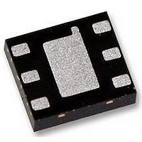
LP5900SD-2.2 National Semiconductor, LP5900SD-2.2 Datasheet - Page 4

LP5900SD-2.2
Manufacturer Part Number
LP5900SD-2.2
Description
V REG, LDO, 100MA, SMD, LLP-6, 5900
Manufacturer
National Semiconductor
Datasheet
1.LP5900SD-2.2.pdf
(12 pages)
Specifications of LP5900SD-2.2
Primary Input Voltage
3.2V
Output Voltage
2.2V
Dropout Voltage Vdo
80mV
No. Of Pins
6
Output Current
150mA
Voltage Regulator Case Style
LLP
Operating Temperature Range
-40°C To +125°C
Output Voltage Fixed
2.2V
Rohs Compliant
Yes
Lead Free Status / RoHS Status
Lead free / RoHS Compliant
www.national.com
V
ΔV
I
I
I
V
I
PSRR
e
T
LOAD
Q
G
SC
n
SHUTDOWN
IN
DO
Symbol
Absolute Maximum Ratings
If Military/Aerospace specified devices are required,
please contact the National Semiconductor Sales Office/
Distributors for availability and specifications.
Electrical Characteristics
Limits in standard typeface are for T
(-40ºC
V
V
V
V
Continuous Power Dissipation
(Note 3)
Junction Temperature (T
Storage Temperature Range
Maximum Lead Temperature
(Soldering, 10 sec.)
ESD Rating (Note 4)
OUT
OUT (NOM)
IN
OUT
EN
Pin: Input Voltage
Pin: Enable Input Voltage
Pin: Output Voltage
≤
T
J
+ 1.0V, V
Input Voltage
Output Voltage Tolerance
Line Regulation
Load Regulation
Load Current
Maximum Output Current
Quiescent Current (Note 11)
Ground Current (Note 13)
Dropout Voltage(Note 10)
Short Circuit Current Limit
Power Supply Rejection Ratio
(Note 15)
Output Noise Voltage
(Note 15)
Thermal Shutdown
≤
+125ºC). Unless otherwise noted, specifications apply to the LP5900 Typical Application Circuit (pg. 1) with: V
EN
Parameter
= 1.2V, C
JMAX
)
IN
-0.3 to (V
-0.3 to (V
= C
A
= 25ºC. Limits in boldface type apply over the full operating junction temperature range
OUT
= 0.47 μF, I
IN
IN
Internally Limited
+ 0.3V) to 6.0V
+ 0.3V) to 6.0V
V
mA to 150mA
V
mA
I
(Note 9)
V
V
V
I
I
(Note 12)
f = 100 Hz, I
f = 1 kHz, I
f = 10 kHz, I
f = 50 kHz, I
f = 100 kHz, I
BW = 10 Hz to 100 kHz,
V
Temperature
Hysteresis
OUT
OUT
OUT
IN
IN
EN
EN
EN
IN
-65 to 150°C
(Notes 1, 2)
-0.3 to 6.0V
= (V
= (V
= 4.2V
= 1.2V, I
= 1.2V, I
= 0.3V (Disabled)
= 1 mA to 150 mA
= 0 mA (V
= 150 mA
OUT(NOM)
OUT(NOM)
150°C
260°C
(max)
(max)
OUT
OUT
OUT
OUT
OUT
= 1.0 mA. (Note 2), (Note 7)
OUT
OUT
OUT
Conditions
OUT
= 150 mA
= 150 mA
= 150 mA
= 150 mA
+ 1.0V) to 5.5V, I
+ 1.0V) to 5.5V, I
= 0 mA
= 150 mA
= 150 mA
4
= 2.5V)
Operating Ratings
Thermal Properties
V
V
Recommended Load Current
(Note 5)
Junction Temperature Range (T
Ambient Temperature Range (T
(Note 5)
Junction to Ambient Thermal Resistance θ
JEDEC Board (LLP-6)(Note 16)
Human Body Model
Machine Model
I
I
I
IN
EN
OUT
OUT
OUT
JEDEC Board (microSMD)
(Note 16)
4L Cellphone Board (microSMD)
: Input Voltage Range
: Enable Voltage Range
= 0 mA
= 1 mA
= 150 mA
OUT
OUT
= 1
= 1
Min
150
2.5
−2
0
(Note 1)
A
J
0.001
0.003
)
)
0.05
Typ
160
300
160
6.5
25
30
80
85
75
65
52
40
10
20
7
,
0 to (V
JA
(Note 2)
-40°C to +125°C
Max
-40°C to +85°C
230
150
5.5
1.0
(Note 6)
50
2
2.5V to 5.5V
IN
0 to 150 mA
5.5V (max)
157.4°C/W
+ 0.3V) to
77.3°C/W
88°C/W
200V
μV
%/mA
Units
2 kV
%/V
mA
mV
mA
IN
µA
µA
dB
ºC
%
V
RMS
=


