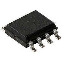
LT3009ESC8-1.5#PBF Linear Technology, LT3009ESC8-1.5#PBF Datasheet - Page 14

LT3009ESC8-1.5#PBF
Manufacturer Part Number
LT3009ESC8-1.5#PBF
Description
IC, LDO VOLT REG, 1.5V, 20mA, SC-70-8
Manufacturer
Linear Technology
Datasheet
1.LT3009ESC8-1.2PBF.pdf
(20 pages)
Specifications of LT3009ESC8-1.5#PBF
Primary Input Voltage
2V
Output Voltage Fixed
1.5V
Dropout Voltage Vdo
280mV
No. Of Pins
8
Output Current
20mA
Operating Temperature Range
-40°C To +125°C
Termination Type
SMD
Msl
MSL 1 - Unlimited
Rohs Compliant
Yes
Lead Free Status / RoHS Status
Lead free / RoHS Compliant
Available stocks
Company
Part Number
Manufacturer
Quantity
Price
LT3009 Series
APPLICATIONS INFORMATION
Voltage and temperature coeffi cients are not the only
sources of problems. Some ceramic capacitors have a
piezoelectric response. A piezoelectric device generates
voltage across its terminals due to mechanical stress,
similar to the way a piezoelectric accelerometer or micro-
phone works. For a ceramic capacitor, the stress can be
induced by vibrations in the system or thermal transients.
The resulting voltages produced can cause appreciable
amounts of noise, especially when a ceramic capacitor is
used for noise bypassing. A ceramic capacitor produced
Figure 4’s trace in response to light tapping from a pencil.
Similar vibration induced behavior can masquerade as
increased output voltage noise.
14
500μV/DIV
V
OUT
Figure 4. Noise Resulting from Tapping
on a Ceramic Capacitor
V
C
I
LOAD
OUT
OUT
= 0.6V
= 22μF
= 10μA
100ms/DIV
3009 F04
Thermal Considerations
The LT3009’s maximum rated junction temperature of
125°C limits its power-handling capability. Two components
comprise the power dissipated by the device:
1. Output current multiplied by the input/output voltage
2. GND pin current multiplied by the input voltage:
GND pin current is found by examining the GND Pin Cur-
rent curves in the Typical Performance Characteristics
section. Power dissipation equals the sum of the two
components listed prior.
The LT3009 regulator has internal thermal limiting designed
to protect the device during overload conditions. For con-
tinuous normal conditions, do not exceed the maximum
junction temperature rating of 125°C. Carefully consider
all sources of thermal resistance from junction to ambi-
ent including other heat sources mounted in proximity to
the LT3009. For surface mount devices, heat sinking is
accomplished by using the heat spreading capabilities of
the PC board and its copper traces. Copper board stiffeners
and plated through-holes can also be used to spread the
heat generated by power devices.
differential: I
I
GND
• V
IN
OUT
• (V
IN
– V
OUT
)
3009fc


