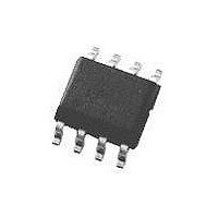
LM2621MM National Semiconductor, LM2621MM Datasheet - Page 3

LM2621MM
Manufacturer Part Number
LM2621MM
Description
IC, STEP-UP DC/DC CONVERTER, 8-SOIC
Manufacturer
National Semiconductor
Datasheet
1.LM2621MMNOPB.pdf
(11 pages)
Specifications of LM2621MM
Primary Input Voltage
14V
No. Of Outputs
1
Output Voltage
14V
Output Current
1A
No. Of Pins
8
Operating Temperature Range
-40°C To +85°C
Power Dissipation Pd
500mW
Lead Free Status / RoHS Status
Contains lead / RoHS non-compliant
Available stocks
Company
Part Number
Manufacturer
Quantity
Price
Part Number:
LM2621MM
Manufacturer:
NS/国半
Quantity:
20 000
Part Number:
LM2621MM(SO6A)
Manufacturer:
NS/国半
Quantity:
20 000
Part Number:
LM2621MMX
Manufacturer:
NS/国半
Quantity:
20 000
Part Number:
LM2621MMX/NOPB
Manufacturer:
NS/国半
Quantity:
20 000
V
V
V
V
V
η
D
I
I
I
R
Enable Section
V
V
DD
SD
CL
IN_ST
IN_OP
FB
OUT_MAX
HYST
EN_LO
EN_HI
DS_ON
Absolute Maximum Ratings
If Military/Aerospace specified devices are required,
please contact the National Semiconductor Sales Office/
Distributors for availability and specifications.
Electrical Characteristics
Limits in standard typeface are for T
−40˚C to +85˚C. Unless otherwise specified: V
Note 1: Absolute maximum ratings indicate limits beyond which damage to the device may occur. Electrical specifications do not apply when operating the device
outside of its rated operating conditions.
Note 2: The maximum power dissipation must be derated at elevated temperatures and is dictated by T
ambient thermal resistance), and T
given in the Absolute Maximum Ratings, whichever is lower.
Note 3: The human body model is a 100 pF capacitor discharged through a 1.5 kΩ resistor into each pin. For Pin 8 (SW) the ESD rating is 1.5 kV.
Note 4: Output in regulation, V
Note 5: This is the hysteresis value of the internal comparator used for the gated-oscillator control scheme.
Note 6: This is the current into the V
Note 7: This is the total current into pins V
Note 8: When the EN pin is below V
Symbol
SW Pin Voltage
BOOT, V
FREQ Pin
θ
T
Storage Temperature Range
Lead Temp. (Soldering, 5 sec)
JA
Jmax
(Note 2)
(Note 2)
DD
, EN and FB Pins
Minimum Start-Up Supply
Voltage (Note 4)
Minimum Operating Supply
Voltage (once started)
FB Pin Voltage
Maximum Output Voltage
Hysteresis Voltage (Note 7)
Efficiency
Switch Duty Cycle
Operating Quiescent Current
(Note 6)
Shutdown Quiescent Current
(Note 7)
Switch Peak Current Limit
MOSFET Switch On
Resistance
EN Pin Voltage Low (Note 8)
EN Pin Voltage High (Note 8)
Parameter
OUT
A
(ambient temperature). The maximum allowable power dissipation at any temperature is P
= V
DD
EN_LO
OUT (NOMINAL
pin.
, the regulator is shut down; when it is above V
DD
, BOOT, SW and FREQ.
J
= 25˚C, and limits in boldface type apply over the full operating temperature range of
−65˚C to +150˚C
)
−0.5 V to 14.5V
±
5%
−0.5V to 10V
Condition
I
I
V
500mA
V
= 200mA
FB Pin
V
5.0V; EN Pin
LOAD
LOAD
DD
(Note 1)
IN
IN
DD
= V
240˚C/W
= 3.6V; V
= 2.5V; V
, BOOT and SW Pins at
= 0mA
= 0mA
100µA
150˚C
260˚C
OUT
>
1.3V; EN Pin at V
= 3.3V.
OUT
OUT
<
200mV
3
= 5V; I
= 3.3V; I
Operating Conditions
Power Dissipation (T
(Note 2)
ESD Rating (Note 3)
V
FB, EN Pins
BOOT Pin
Ambient Temperature (T
DD
LOAD
EN_HI
LOAD
Pin
DD
, the regulator is operating.
=
jmax
0.65
1.24
0.01
2.85
0.17
Typ
1.1
14
30
87
87
70
80
(maximum junction temperature), θ
A
=25˚C)
A
)
0.7V
1.2028
Min
60
dmax
DD
= (T
(Note 1)
jmax
0.15V
1.2772
- T
Max
110
1.2
2.5
45
80
−40˚C to +85˚C
A
)/ θ
DD
JA
2.5V to 5V
www.national.com
JA
or the number
0 to V
0 to 10V
500mW
(junction to
Units
mV
2kV
µA
µA
%
%
Ω
V
V
V
V
A
V
V
DD


