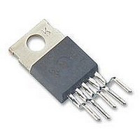
SI-8008HFE Allegro Microsystems Inc, SI-8008HFE Datasheet - Page 6
SI-8008HFE
Manufacturer Part Number
SI-8008HFE
Description
IC, BUCK, REG, 5.5A, 5TO220
Manufacturer
Allegro Microsystems Inc
Datasheet
1.SI-8008HFE.pdf
(10 pages)
Specifications of SI-8008HFE
Primary Input Voltage
40V
No. Of Outputs
1
Output Voltage
24V
Output Current
5.5A
Voltage Regulator Case Style
No. Of Pins
Operating Temperature Range
-30°C To +85°C
Base
RoHS Compliant
Package / Case
TO220
Available stocks
Company
Part Number
Manufacturer
Quantity
Price
Company:

Part Number:
SI-8008HFE
Manufacturer:
IR
Quantity:
4 000
Part Number:
SI-8008HFE
Manufacturer:
SANKEN
Quantity:
20 000


SI-8008HFE
Diode Di A Schottky-barrier diode must be used for Di. If other
diode types are used, such as fast recovery diodes, the IC may be
destroyed because of the reverse voltage applied by the recovery
voltage or ON voltage.
Choke Coil L1 If the winding resistance of the choke coil is too
high, the efficiency may be reduced below rating. Because the
overcurrent protection start current is approximately 6.5 A, atten-
tion must be paid to the heating of the choke coil by magnetic
saturation due to overload or short-circuited load.
Capacitors C1, C2, C3, and C4 Because for SMPS, large
ripple currents flow across C1 and C2, capacitors with high
frequency and low impedance must be used. If the impedance of
C2 is too high, the switching waveform may not be normal at low
temperatures. Do not use either OS or tantalum types of capaci-
GND
V
IN
C1
C4
1
IN
SS
SI-8008HFE
5
C3
Soft Start Only
GND
3
ADJ
SW
All external components should be mounted as close as possible
to the SI-8008HFE. The ground of all components should be
connected at one point.
2
4
Vin
Di
115 Northeast Cutoff, Box 15036
Allegro MicroSystems, Inc.
Worcester, Massachusetts 01615-0036 (508) 853-5000
www.allegromicro.com
L1
Vin
C1
C1
R1
R2
Component Selection
Typical Application Diagram
Recommended PCB Layout
C4
I
ADJ
Vsw
D1
D1
C4
U1
L1
R2
Vsw
C2
V
GND
GND
O
U1
R2
GND
GND
GND
L1
R1
tors for C2, because those cause an abnormal oscillation.
The device is stabilized, and for proper operation, C1 and C4
must be located close to the device (see layout diagram, below).
C3 is required only if the soft start function is used. If not using
soft start, leave the SS terminal open. A pull-up resistor is pro-
vided inside the IC.
Resistor Bridge R1 and R2 comprise the resistor bridge for the
output voltage, V
I
present to ensure stable operation, even if V
is, even if there is no R1). V
DC-to-DC Step-Down Converter
ADJ
R1
C2
should always be set to 1 mA. Note that R2 should always be
R1
Vadj/Vos
C2
=
(
Vadj/Vos
V
O
−
I
ADJ
V
ADJ
Component
C3
C3
) (
=
O
Vout
Vout
C1
C2
C3
C4
L1
Di
, and are calculated as follows:
S1
S1
V
1
O
×
−
10
0
8 .
−
3
) ) , and
(
1500 μF
1000 μF
0.1 μF (For soft start function)
4.7 μF (RPER11H475K5)
FMB-G16L (Sanken)
100 μH
Ω
O
should be at least V
R2
=
V
I
ADJ
ADJ
Rating
O
, is set to 0.8 V (that
=
1
×
0
10
IN
8 .
−
+ 8%.
3
=
0
8 .
(
k
Ω
)
6
Related parts for SI-8008HFE
Image
Part Number
Description
Manufacturer
Datasheet
Request
R

Part Number:
Description:
Switch, Safety, Magnet Sensor, 30' Cable(Used w/SI-MAG2MM Magnet, GM-FA-10J Ctrl)
Manufacturer:
BANNER ENGINEERING
Datasheet:

Part Number:
Description:
CONN MAGJACK 1PT 10/100BTX G/Y
Manufacturer:
Stewart Connector
Datasheet:

Part Number:
Description:
CONN MAGJACK 1PORT SHLD GIGABIT
Manufacturer:
Stewart Connector
Datasheet:

Part Number:
Description:
CONN MAGJACK 1PT GIGABIT G/G
Manufacturer:
Stewart Connector
Datasheet:
Part Number:
Description:
CONN MAGJACK 1PT GIGABIT G/Y
Manufacturer:
Stewart Connector
Datasheet:
Part Number:
Description:
CONN MAGJACK 1PT GIGABIT SHLD
Manufacturer:
Stewart Connector
Datasheet:
Part Number:
Description:
CONN MAGJACK 1PT GIGABIT SHLD
Manufacturer:
Stewart Connector
Datasheet:
Part Number:
Description:
CONN MAGJACK 1PT GIGABIT SHLD
Manufacturer:
Stewart Connector
Datasheet:
Part Number:
Description:
CONN MAGJACK 1PT GIGABIT SHLD
Manufacturer:
Stewart Connector
Datasheet:
Part Number:
Description:
CONN MAGJACK 1PT GIGABIT G/G
Manufacturer:
Stewart Connector
Datasheet:

Part Number:
Description:
IC, LINEAR VOLTAGE REGULATOR 5V TO-220-5
Manufacturer:
Allegro Microsystems Inc
Datasheet:

Part Number:
Description:
Regulator IC - Low Dropout Voltage (Surface Mount)
Manufacturer:
Allegro Microsystems Inc
Datasheet:
Part Number:
Description:
Regulator IC - Low Dropout Voltage (Surface Mount)
Manufacturer:
Allegro Microsystems Inc
Datasheet:
Part Number:
Description:
Regulator IC - Low Dropout Voltage (Surface Mount)
Manufacturer:
Allegro Microsystems Inc
Datasheet:
Part Number:
Description:
Regulator IC - Low Dropout Voltage (Surface Mount)
Manufacturer:
Allegro Microsystems Inc