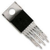
LM2678T-ADJ National Semiconductor, LM2678T-ADJ Datasheet - Page 13

LM2678T-ADJ
Manufacturer Part Number
LM2678T-ADJ
Description
SWITCHING REG 5A ADJ, 2678, TO2207
Manufacturer
National Semiconductor
Datasheet
1.LM2678T-ADJ.pdf
(27 pages)
Specifications of LM2678T-ADJ
Primary Input Voltage
40V
No. Of Outputs
1
Output Voltage
37V
Output Current
5A
Voltage Regulator Case Style
TO-220
No. Of Pins
7
Operating Temperature Range
-40°C To +125°C
Svhc
No SVHC
Lead Free Status / RoHS Status
Lead free / RoHS Compliant
Available stocks
Company
Part Number
Manufacturer
Quantity
Price
Company:
Part Number:
LM2678T-ADJ
Manufacturer:
NS
Quantity:
5 510
Part Number:
LM2678T-ADJ
Manufacturer:
NS/国半
Quantity:
20 000
Part Number:
LM2678T-ADJ/NOPB
Manufacturer:
TI/德州仪器
Quantity:
20 000
Application Hints
Using the nomographs and tables in this data sheet (or use
the available design software at http://www.national.com) a
complete step-down regulator can be designed in a few
simple steps.
Step 1: Define the power supply operating conditions:
Required output voltage
Maximum DC input voltage
Maximum output load current
Step 2: Set the output voltage by selecting a fixed output
LM2678 (3.3V, 5V or 12V applications) or determine the
required feedback resistors for use with the adjustable
LM2678−ADJ
Step 3: Determine the inductor required by using one of the
four nomographs, Figure 3 through Figure 6. Table 1 pro-
vides a specific manufacturer and part number for the induc-
tor.
Step 4: Using Table 3 (fixed output voltage) or Table 6
(adjustable output voltage), determine the output capaci-
tance required for stable operation. Table 2 provides the
specific capacitor type from the manufacturer of choice.
Step 5: Determine an input capacitor from Table 4 for fixed
output voltage applications. Use Table 2 to find the specific
capacitor type. For adjustable output circuits select a capaci-
tor from Table 2 with a sufficient working voltage (WV) rating
greater than Vin max, and an rms current rating greater than
one-half the maximum load current (2 or more capacitors in
parallel may be required).
Step 6: Select a diode from Table 5. The current rating of the
diode must be greater than I load max and the Reverse
Voltage rating must be greater than Vin max.
Step 7: Include a 0.01µF/50V capacitor for Cboost in the
design.
FIXED OUTPUT VOLTAGE DESIGN EXAMPLE
A system logic power supply bus of 3.3V is to be generated
from a wall adapter which provides an unregulated DC volt-
age of 13V to 16V. The maximum load current is 4A.
Through-hole components are preferred.
Step 1: Operating conditions are:
Vout = 3.3V
Vin max = 16V
Iload max = 4A
Step 2: Select an LM2678T-3.3. The output voltage will have
a tolerance of
temperature range.
Step 3: Use the nomograph for the 3.3V device ,Figure 3.
The intersection of the 16V horizontal line (V
4A vertical line (I
tor, is required.
From Table 1, L46 in a through-hole component is available
from Renco with part number RL-1283-15-43.
Step 4: Use Table 3 to determine an output capacitor. With a
3.3V output and a 15µH inductor there are four through-hole
output capacitor solutions with the number of same type
capacitors to be paralleled and an identifying capacitor code
given. Table 2 provides the actual capacitor characteristics.
Any of the following choices will work in the circuit:
2 x 220µF/10V Sanyo OS-CON (code C5)
2 x 820µF/16V Sanyo MV-GX (code C5)
1 x 3900µF/10V Nichicon PL (code C7)
±
2% at room temperature and
load
max) indicates that L46, a 15µH induc-
(Continued)
±
3% over the full operating
in
max) and the
13
2 x 560µF/35V Panasonic HFQ (code C5)
Step 5: Use Table 4 to select an input capacitor. With 3.3V
output and 15µH there are three through-hole solutions.
These capacitors provide a sufficient voltage rating and an
rms current rating greater than 2A (1/2 I
using Table 2 for specific component characteristics the
following choices are suitable:
2 x 680µF/63V Sanyo MV-GX (code C13)
1 x 1200µF/63V Nichicon PL (code C25)
1 x 1500µF/63V Panasonic HFQ (code C16)
Step 6: From Table 5 a 5A or more Schottky diode must be
selected. For through-hole components only 40V rated di-
odes are indicated and 4 part types are suitable:
1N5825
MBR745
80SQ045
6TQ045
Step 7: A 0.01µF capacitor will be used for Cboost.
ADJUSTABLE OUTPUT DESIGN EXAMPLE
In this example it is desired to convert the voltage from a two
battery automotive power supply (voltage range of 20V to
28V, typical in large truck applications) to the 14.8VDC alter-
nator supply typically used to power electronic equipment
from single battery 12V vehicle systems. The load current
required is 3.5A maximum. It is also desired to implement the
power supply with all surface mount components.
Step 1: Operating conditions are:
Vout = 14.8V
Vin max = 28V
Iload max = 3.5A
Step 2: Select an LM2678S-ADJ. To set the output voltage
to 14.9V two resistors need to be chosen (R1 and R2 in
Figure 2). For the adjustable device the output voltage is set
by the following relationship:
Where V
A recommended value to use for R1 is 1K. In this example
then R2 is determined to be:
R2 = 11.23KΩ
The closest standard 1% tolerance value to use is 11.3KΩ
This will set the nominal output voltage to 14.88V which is
within 0.5% of the target value.
Step 3: To use the nomograph for the adjustable device,
Figure
Volt • microsecond constant (E • T expressed in V • µS) from
the following formula:
where V
switch which is R
be typically 0.12Ω x 3.5A or 0.42V and V
across the forward bisased Schottky diode, typically 0.5V.
SAT
FB
6,
is the feedback voltage of typically 1.21V.
is the voltage drop across the internal power
requires
ds(ON)
times I
a
calculation
load
. In this example this would
D
of
is the voltage drop
load
the
max). Again
www.national.com
inductor


