LM2592HVT-3.3 National Semiconductor, LM2592HVT-3.3 Datasheet - Page 8
LM2592HVT-3.3
Manufacturer Part Number
LM2592HVT-3.3
Description
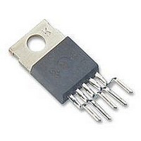
SWITCHING REG 2A 3.3V, 2592, TO-220
Manufacturer
National Semiconductor
Datasheet
1.LM2592HVT-3.3.pdf
(20 pages)
Specifications of LM2592HVT-3.3
Primary Input Voltage
12V
No. Of Outputs
1
Output Voltage
3.3V
Output Current
2A
Voltage Regulator Case Style
TO-220
No. Of Pins
5
Operating Temperature Range
-40°C To +125°C
Svhc
No SVHC
Lead Free Status / RoHS Status
Lead free / RoHS Compliant


www.national.com
Test Circuit and Layout Guidelines
Component Values shown are for V
V
C
C
D1
L1
Select R
Component Values shown are for V
V
C
C
D1 — 3.3A, 60V Schottky Rectifier, 31DQ06 (International Rectifier)
L1 — 47 µH, See Inductor Selection Procedure
R
R
C
Typical Values
C
C
R
drag feedback pin below ground). Required if V
†
OUT
IN
OUT
OUT
IN
OUT
1
2
FF
SS
DELAY
PULL UP
Small signal Schottky diode to prevent damage to feedback pin by negative spike when output is shorted (C
:
— 1 k , 1%
— 7.15k, 1%
— 0.1 µF
— 3.3 nF
—
—
:
= 5V, I
—
= 10V, I
— 470 µF, 35V, Aluminum Electrolytic Nichicon “PM Series”
— 0.1 µF
—
1
— 220 µF, 35V Aluminum Electrolytic, Nichicon “PM Series”
33 µH, See Inductor Selection Procedure
3.3A, 60V Schottky Rectifier, 31DQ06 (International Rectifier)
to be approximately 1 k , use a 1% resistor for best stability.
— 4.7k (use 22k if V
470 µF, 50V, Aluminum Electrolytic Nichicon “PM Series”
LOAD
220 µF, 25V Aluminum Electrolytic, Nichicon “PM Series”
LOAD
= 2A.
= 2A.
OUT
IN
IN
is
= 15V,
= 20V,
45V)
FIGURE 1. Standard Test Circuits and Layout Guides
IN
>
40V
Adjustable Output Voltage Versions
Fixed Output Voltage Versions
8
FF
not being able to discharge immediately will
10129425
10129424
Related parts for LM2592HVT-3.3
Image
Part Number
Description
Manufacturer
Datasheet
Request
R

Part Number:
Description:
National Semiconductor [8-Bit D/A Converter]
Manufacturer:
National Semiconductor
Datasheet:
Part Number:
Description:
National Semiconductor [Media Coprocessor]
Manufacturer:
National Semiconductor
Datasheet:
Part Number:
Description:
Digitally Controlled Tone and Volume Circuit with Stereo Audio Power Amplifier, Microphone Preamp Stage and National 3D Sound
Manufacturer:
National Semiconductor
Datasheet:
Part Number:
Description:
Digitally Controlled Tone and Volume Circuit with Stereo Audio Power Amplifier, Microphone Preamp Stage and National 3D Sound
Manufacturer:
National Semiconductor
Datasheet:
Part Number:
Description:
AC97 Rev 2 Codec with Sample Rate Conversion and National 3D Sound
Manufacturer:
National Semiconductor
Part Number:
Description:
Manufacturer:
National Semiconductor
Datasheet:
Part Number:
Description:
Manufacturer:
National Semiconductor
Datasheet:
Part Number:
Description:
General Purpose, Low Voltage, Low Power, Rail-to-Rail Output Operational Amplifiers
Manufacturer:
National Semiconductor
Datasheet:
Part Number:
Description:
8-bit 20 MSPS flash A/D converter.
Manufacturer:
National Semiconductor
Datasheet:
Part Number:
Description:
Low Noise Quad Operational Amplifier
Manufacturer:
National Semiconductor
Datasheet:
Part Number:
Description:
Quad Differential Line Receivers
Manufacturer:
National Semiconductor
Datasheet:
Part Number:
Description:
Quad High Speed Trapezoidal? Bus Transceiver
Manufacturer:
National Semiconductor
Datasheet:
Part Number:
Description:
Dual Line Receiver
Manufacturer:
National Semiconductor
Datasheet:
Part Number:
Description:
TTL to 10k ECL Level Translator with Latch
Manufacturer:
National Semiconductor
Datasheet: