LM22678TJ-ADJ National Semiconductor, LM22678TJ-ADJ Datasheet
LM22678TJ-ADJ
Specifications of LM22678TJ-ADJ
Available stocks


Related parts for LM22678TJ-ADJ

LM22678TJ-ADJ Summary of contents
Page 1
... The LM22678 series also has built in thermal shutdown, current limiting and an enable control input that can power down the regulator to a low 25 µA quiescent current standby condition. Simplified Application Schematic © 2008 National Semiconductor Corporation Features ■ Wide input voltage range: 4.5V to 42V ■ ...
Page 2
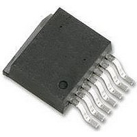
... Connection Diagram Ordering Information Output Voltage Order Number ADJ LM22678TJE-ADJ ADJ LM22678TJ-ADJ 5.0 LM22678TJE-5.0 5.0 LM22678TJ-5.0 Pin Descriptions Pin Name Description 1 SW Switch pin 2 VIN Source input voltage 3 BOOT Bootstrap input 4 GND System ground 5 NC Not connected 6 FB Feedback pin 7 EN Precision enable pin www ...
Page 3
... Absolute Maximum Ratings If Military/Aerospace specified devices are required, please contact the National Semiconductor Sales Office/ Distributors for availability and specifications. VIN to GND EN Pin Voltage SW to GND (Note 2) BOOT Pin Voltage FB Pin Voltage Power Dissipation Junction Temperature Electrical Characteristics junction temperature (T ) range of -40°C to +125°C. Minimum and Maximum limits are guaranteed through test, design, or statistical J correlation ...
Page 4
Note 1: Absolute Maximum Ratings indicate limits beyond which damage to the device may occur, including inoperability and degradation of device reliability and/or performance. Functional operation of the device and/or non-degradation at the Absolute Maximum Ratings or other conditions beyond ...
Page 5
Feedback Bias Current vs Temperature Standby Quiescent Current vs Input Voltage Normalized Feedback Voltage vs Input Voltage Normalized Enable Threshold Voltage vs Temperature 30076105 Normalized Feedback Voltage vs Temperature 30076106 30076109 5 30076110 30076107 www.national.com ...
Page 6
Typical Application Circuit and Block Diagram www.national.com FIGURE 1. 3. OUT 6 30076114 ...
Page 7
Detailed Operating Description The LM22678 switching regulator features all of the functions necessary to implement an efficient high voltage buck regu- lator using a minimum of external components. This easy to use regulator integrates a 42V N-Channel switch with an ...
Page 8
Boot Pin The LM22678 integrates an N-Channel FET switch and as- sociated floating high voltage level shift / gate driver. This gate driver circuit works in conjunction with an internal diode and an external bootstrap capacitor. A 0.01 µF ceramic ...
Page 9
RMS current and minimum ripple voltage. A good ap- RMS proximation for the required ripple current rating necessary is I > RMS OUT Quality ceramic capacitors with a low ESR should be selected for the ...
Page 10
Circuit Board Layout Board layout is critical for switching power supplies. First, the ground plane area must be sufficient for thermal dissipation purposes. Second, appropriate guidelines must be followed to reduce the effects of switching noise. Switch mode con- verters ...
Page 11
PCB Layout Example 30076125 11 www.national.com ...
Page 12
Schematic for Buck/Boost (Inverting) Application See AN-1888 for more information on the inverting (buck- boost) application generating a negative output voltage from a positive input voltage. www.national.com 30076126 12 ...
Page 13
Physical Dimensions inches (millimeters) unless otherwise noted 7-Lead Plastic TO-263 THIN Package NS Package Number TJ7A 13 www.national.com ...
Page 14
... For more National Semiconductor product information and proven design tools, visit the following Web sites at: Products Amplifiers www.national.com/amplifiers Audio www.national.com/audio Clock Conditioners www.national.com/timing Data Converters www.national.com/adc Displays www.national.com/displays Ethernet www.national.com/ethernet Interface www.national.com/interface LVDS www.national.com/lvds Power Management www.national.com/power Switching Regulators www.national.com/switchers LDOs www ...