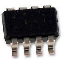
LM22673MR-ADJ National Semiconductor, LM22673MR-ADJ Datasheet - Page 8

LM22673MR-ADJ
Manufacturer Part Number
LM22673MR-ADJ
Description
REGULATOR, ADJ. VOLTAGE, 3A 8PSOP
Manufacturer
National Semiconductor
Datasheet
1.LM22673MR-ADJ.pdf
(16 pages)
Specifications of LM22673MR-ADJ
Primary Input Voltage
42V
No. Of Outputs
1
Output Current
3A
Voltage Regulator Case Style
PSOP
No. Of Pins
8
Operating Temperature Range
-40°C To +125°C
Svhc
No SVHC (15-Dec-2010)
Package /
RoHS Compliant
Available stocks
Company
Part Number
Manufacturer
Quantity
Price
Company:
Part Number:
LM22673MR-ADJ/NOPB
Manufacturer:
NS
Quantity:
475
Company:
Part Number:
LM22673MR-ADJ/NOPB
Manufacturer:
NS/TI
Quantity:
3 600
www.national.com
Detailed Operating Description
The LM22673 switching regulator features all of the functions
necessary to implement an efficient high voltage buck regu-
lator using a minimum of external components. This easy to
use regulator integrates a 42V N-Channel switch with an out-
put current capability of 3A. The regulator control method is
based on voltage mode control with input voltage feed for-
ward. The loop compensation is integrated into the LM22673
so that no external compensation components need to be se-
lected or utilized. Voltage mode control offers short minimum
on-times allowing short duty-cycles necessary in high input
voltage applications. The operating frequency is fixed at 500
kHz to allow for small external components while avoiding
excessive switching losses. The output voltage can be set as
low as 1.285V with the -ADJ device. Fault protection features
include current limiting and thermal shutdown. The device is
available in the TO-263 THIN and PSOP packages featuring
an exposed pad to aid thermal dissipation.
The functional block diagram with typical application of the
LM22673 is shown in Figure 1.
The internal compensation of the -ADJ option of the LM22673
is optimized for output voltages up to 5V. If an output voltage
of 5V or higher is needed, the -5.0 fixed output voltage option
with an additional external resistive feedback voltage divider
may also be used.
Maximum Duty-Cycle / Dropout
Voltage
The typical maximum duty-cycle is 85%. This corresponds to
a typical minimum off-time of 300 ns. This forced off-time is
important to provide enough time for the Cboot capacitor to
charge during each cycle. The lowest input voltage required
to maintain operation is:
Where V
Schottky diode and V
power N-FET of the LM22673. The R
specified in the electrical characteristics section of this
datasheet to calculate V
the switching frequency.
Minimum Duty-Cycle
Besides a minimum off-time, there is also a minimum on-time
which will take effect when the output voltage is adjusted very
low and the input voltage is very high. Should the operation
require a shorter minimum on-time than the typical 100 ns,
individual switching pulses will be skipped.
where D is the duty-cycle.
Current Limit
When the power switch turns on, the slight capacitance load-
ing of the Schottky diode, D1, causes a leading-edge current
spike with an extended ringing period. This spike can cause
the current limit comparator to trip prematurely. A leading
D
is the forward voltage drop across the re-circulating
Q
is the voltage drop across the internal
Q
according to the FET current. F is
DS(ON)
of the FET is
8
edge blanking time (T
sampling the spike.
A key feature of the LM22673 is the ability to control the peak
switch current limit. Without this feature, the peak switch cur-
rent would be internally set to 4.2A (typical) to accommodate
3A load current designs. The high current limit requires that
both the inductor (which could saturate with excessively high
currents) and the catch diode be able to safely handle up to
4.2A under load fault condition.
If an application requires a load current less than 3A, the peak
switch current can be set to a limit just over the maximum load
current with the addition of a single programming resistor.
This allows the use of lower rated and more cost effective
inductors and diodes. A resistance of 10 kΩ sets the current
limit to typically 4.8A (typical) peak current and 20 kΩ reduces
the maximum peak current to 2A (typical).
When the switch current reaches the current limit threshold,
the switch is immediately turned off and the internal switching
frequency is reduced. This extends the off time of the switch
to prevent a steady state high current condition. As the switch
current falls below the current limit threshold, the switch cur-
rent will attempt to turn on. If a load fault continues, the switch
will again exceed the threshold and turn off. This will result in
a low duty-cycle pulsing of the power switch to minimize the
overall fault condition power dissipation.
The switching frequency will reduce (fold back) if the overload
condition causes the output voltage to be 72.4% (typical) of
the adjusted output voltage.
The current limit will only protect the inductor from a runaway
condition if the LM22673 is operating in its safe operating
area. A runaway condition of the inductor is potentially catas-
trophic to the application. For every design, the safe operating
area needs to be calculated. Factors in determining the safe
operating area are the switching frequency, input voltage,
output voltage, minimum on-time and feedback voltage dur-
ing an over current condition.
As a first pass check, if the following equation holds true, a
given design is considered in a safe operating area and the
current limit will protect the circuit:
If the equation above does not hold true, the following sec-
ondary equation will need to hold true to be in safe operating
area:
FIGURE 2. Peak Current Limit vs IADJ Resistor
V
IN
x T
BLK
BLK
) of 110 ns (typical) is used to avoid
x F < V
OUT
x 0.724
30076213


