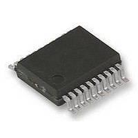
LM20333MH National Semiconductor, LM20333MH Datasheet - Page 16

LM20333MH
Manufacturer Part Number
LM20333MH
Description
BUCK REG, 3A, ADJ, POWERWISE, 20TSSOP
Manufacturer
National Semiconductor
Datasheet
1.LM20333MH.pdf
(20 pages)
Specifications of LM20333MH
Primary Input Voltage
36V
No. Of Outputs
1
Output Voltage
32V
Output Current
3A
Voltage Regulator Case Style
TSSOP
No. Of Pins
20
Operating Temperature Range
-40°C To +125°C
Svhc
No SVHC
Lead Free Status / RoHS Status
Lead free / RoHS Compliant
Available stocks
Company
Part Number
Manufacturer
Quantity
Price
Part Number:
LM20333MH
Manufacturer:
NS/国半
Quantity:
20 000
Part Number:
LM20333MHX
Manufacturer:
NS/国半
Quantity:
20 000
www.national.com
The dashed lines in the figures above show an approximation
of the minimum and maximum duty cycle limitations; while,
the solid lines define areas of operation for a given ambient
temperature. This data for the figure was derived assuming
the device is operating at 3A continuous output current on a
4 layer PCB with a copper area greater than 4 square inches
exhibiting a thermal characteristic less than 27 °C/W. Since
the internal losses are dominated by the FETs a slight reduc-
tion in current by 500mA allows for much larger regions of
operation, as shown in Figure 11.
Figure 12, shown below, provides a better approximation of
the θ
test consisted of 4 layers: 1oz. copper was used for the inter-
nal layers while the external layers were plated to 2oz. copper
weight. To provide an optimal thermal connection, a 5 x 4 ar-
ray of 12 mil thermal vias located under the thermal pad was
used to connect the 4 layers.
FIGURE 11. Safe Thermal Operating Areas (I
FIGURE 10. Safe Thermal Operating Areas (I
JA
for a given PCB copper area. The PCB used in this
f
f
SW
SW
= 750kHz)
= 500kHz)
30051689
30051691
OUT
OUT
= 2.5A,
= 3A,
16
PCB LAYOUT CONSIDERATIONS
PC board layout is an important part of DC-DC converter de-
sign. Poor board layout can disrupt the performance of a DC-
DC converter and surrounding circuitry by contributing to EMI,
ground bounce, and resistive voltage loss in the traces. These
can send erroneous signals to the DC-DC converter resulting
in poor regulation or instability.
Good layout can be implemented by following a few simple
design rules.
1. Minimize area of switched current loops. In a buck regulator
there are two loops where currents are switched at high slew
rates. The first loop starts from the input capacitor, to the reg-
ulator VIN pin, to the regulator SW pin, to the inductor then
out to the output capacitor and load. The second loop starts
from the output capacitor ground, to the regulator GND pins,
to the inductor and then out to the load (see Figure 13). To
minimize both loop areas the input capacitor should be placed
as close as possible to the VIN pin. Grounding for both the
input and output capacitor should consist of a small localized
top side plane that connects to GND and the exposed pad
(EP). The inductor should be placed as close as possible to
the SW pin and output capacitor.
2. Minimize the copper area of the switch node. Since the
LM20333 has the SW pins on opposite sides of the package
it is recommended that the SW pins should be connected with
a trace that runs around the package. The inductor should be
placed at an equal distance from the SW pins using 100 mil
wide traces to minimize capacitive and conductive losses.
3. Have a single point ground for all device grounds located
under the EP. The ground connections for the compensation,
feedback, and soft-start components should be connected
together then routed to the EP pin of the device. The AGND
pin should connect to GND under the EP. If not properly han-
dled poor grounding can result in degraded load regulation or
erratic switching behavior.
4. Minimize trace length to the FB pin. Since the feedback
node can be high impedance the trace from the output resistor
divider to FB pin should be as short as possible. This is most
important when high value resistors are used to set the output
voltage. The feedback trace should be routed away from the
SW pin and inductor to avoid contaminating the feedback sig-
nal with switch noise.
5. Make input and output bus connections as wide as possi-
ble. This reduces any voltage drops on the input or output of
FIGURE 12. Thermal Resistance vs PCB Area (4 Layer
Board)
30051687


