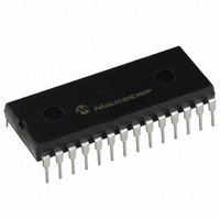
PIC16C55-XT/P Microchip Technology, PIC16C55-XT/P Datasheet - Page 13

PIC16C55-XT/P
Manufacturer Part Number
PIC16C55-XT/P
Description
IC, 8BIT MCU, PIC16C, 4MHZ, DIP-28
Manufacturer
Microchip Technology
Series
PIC® 16Cr
Datasheet
1.PIC16LC58B-04P.pdf
(194 pages)
Specifications of PIC16C55-XT/P
Controller Family/series
PIC16C
No. Of I/o's
20
Ram Memory Size
24Byte
Cpu Speed
4MHz
No. Of Timers
1
Core Size
8 Bit
Program Memory Size
0.5 Kwords
Core Processor
PIC
Speed
4MHz
Peripherals
POR, WDT
Number Of I /o
20
Program Memory Type
OTP
Ram Size
24 x 8
Voltage - Supply (vcc/vdd)
3 V ~ 6.25 V
Oscillator Type
External
Operating Temperature
0°C ~ 70°C
Package / Case
28-DIP (0.600", 15.24mm)
Processor Series
PIC16C
Core
PIC
Data Bus Width
8 bit
Data Ram Size
24 B
Maximum Clock Frequency
40 MHz
Number Of Programmable I/os
20
Number Of Timers
1
Maximum Operating Temperature
+ 70 C
Mounting Style
Through Hole
3rd Party Development Tools
52715-96, 52716-328, 52717-734
Development Tools By Supplier
ICE2000
Minimum Operating Temperature
0 C
Data Rom Size
512 B
Height
4.95 mm
Length
39.75 mm
Supply Voltage (max)
6.25 V
Supply Voltage (min)
3 V
Width
14.73 mm
Lead Free Status / RoHS Status
Lead free / RoHS Compliant
For Use With
XLT28XP - SOCKET TRANSITION ICE 28DIPAC164001 - MODULE SKT PROMATEII 18/28DIP
Eeprom Size
-
Data Converters
-
Connectivity
-
Lead Free Status / Rohs Status
Details
Available stocks
Company
Part Number
Manufacturer
Quantity
Price
Company:
Part Number:
PIC16C55-XT/P
Manufacturer:
MICROCHIP
Quantity:
16
- Current page: 13 of 194
- Download datasheet (3Mb)
TABLE 3-1:
Legend: I = input, O = output, I/O = input/output, P = power, — = Not Used, TTL = TTL input, ST = Schmitt Trigger
OSC2/CLKOUT
2002 Microchip Technology Inc.
OSC1/CLKIN
MCLR/V
Pin Name
T0CKI
RA0
RA1
RA2
RA3
RB0
RB1
RB2
RB3
RB4
RB5
RB6
RB7
V
V
DD
SS
input
PP
PINOUT DESCRIPTION - PIC16C54, PIC16CR54, PIC16C56, PIC16CR56, PIC16C58,
PIC16CR58
DIP
17
18
10
11
12
13
16
15
14
1
2
6
7
8
9
3
4
5
Pin Number
SOIC SSOP Type
17
18
10
12
13
16
15
14
11
1
2
6
7
8
9
3
4
5
15,16
5,6
19
20
10
12
13
14
18
17
11
1
2
7
8
9
3
4
Pin
I/O
I/O
I/O
I/O
I/O
I/O
I/O
I/O
I/O
I/O
I/O
I/O
O
P
P
I
I
I
Preliminary
Buffer
Type
TTL
TTL
TTL
TTL
TTL
TTL
TTL
TTL
TTL
TTL
TTL
TTL
ST
ST
ST
—
—
—
Bi-directional I/O port
Bi-directional I/O port
Clock input to Timer0. Must be tied to V
use, to reduce current consumption.
Master clear (RESET) input/programming voltage input.
This pin is an active low RESET to the device. Voltage on
the MCLR/V
tended entering of Programming mode.
Oscillator crystal input/external clock source input.
Oscillator crystal output. Connects to crystal or resonator
in crystal Oscillator mode. In RC mode, OSC2 pin outputs
CLKOUT, which has 1/4 the frequency of OSC1 and
denotes the instruction cycle rate.
Positive supply for logic and I/O pins.
Ground reference for logic and I/O pins.
PP
pin must not exceed V
Description
PIC16C5X
DD
SS
DS30453D-page 11
to avoid unin-
or V
DD,
if not in
Related parts for PIC16C55-XT/P
Image
Part Number
Description
Manufacturer
Datasheet
Request
R

Part Number:
Description:
IC MCU OTP 512X12 28SOIC
Manufacturer:
Microchip Technology
Datasheet:

Part Number:
Description:
IC MCU OTP 512X12 28SOIC
Manufacturer:
Microchip Technology
Datasheet:

Part Number:
Description:
IC MCU OTP 512X12 28DIP
Manufacturer:
Microchip Technology
Datasheet:

Part Number:
Description:
IC MCU OTP 512X12 28DIP
Manufacturer:
Microchip Technology
Datasheet:

Part Number:
Description:
IC MCU OTP 512X12 28SOIC
Manufacturer:
Microchip Technology
Datasheet:

Part Number:
Description:
IC MCU OTP 512X12 28SOIC
Manufacturer:
Microchip Technology
Datasheet:

Part Number:
Description:
IC MCU OTP 512X12 28SSOP
Manufacturer:
Microchip Technology
Datasheet:

Part Number:
Description:
IC MCU OTP 512X12 28SOIC
Manufacturer:
Microchip Technology
Datasheet:

Part Number:
Description:
IC MCU OTP 512X12 28DIP
Manufacturer:
Microchip Technology
Datasheet:

Part Number:
Description:
IC MCU OTP 512X12 28SOIC
Manufacturer:
Microchip Technology
Datasheet:

Part Number:
Description:
IC MCU OTP 512X12 28SSOP
Manufacturer:
Microchip Technology
Datasheet:

Part Number:
Description:
IC MCU OTP 512X12 28SOIC
Manufacturer:
Microchip Technology
Datasheet:

Part Number:
Description:
IC MCU OTP 512X12 28SSOP
Manufacturer:
Microchip Technology
Datasheet:

Part Number:
Description:
IC MCU OTP 512X12 28DIP
Manufacturer:
Microchip Technology
Datasheet:

Part Number:
Description:
IC MCU OTP 512X12 28SOIC
Manufacturer:
Microchip Technology
Datasheet:


