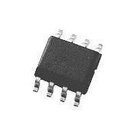
FM25640-G Ramtron, FM25640-G Datasheet

FM25640-G
Specifications of FM25640-G
Available stocks
Related parts for FM25640-G
FM25640-G Summary of contents
Page 1
... Grade 3 AEC-Q100 Qualified (-G) Pin Configuration VSS Pin Names /CS product offers /HOLD /WP SCK SI SO VDD VSS Ordering Information FM25640-G FM25640-GTR drop-in FM25640-S * FM25640-STR * * End of life. Last time buy June 2009. VDD 1 8 HOLD 2 7 SCK Function Chip Select Hold Write Protect ...
Page 2
... SO can be connected to SI for a single pin data interface since the part communicates in half-duplex. VDD Supply Supply Voltage: 5V VSS Supply Ground Rev. 3.2 Feb. 2011 13 Counter Data I/O Register Nonvolatile Status Figure 1. Block Diagram FM25640 2,048 x 32 FRAM Array Register ...
Page 3
... While there are four such modes, the FM25640 supports modes 0 and 3. Figure 4 shows the required signal relationships for modes 0 and 3. In both cases, data is clocked into the FM25640 on the rising edge of SCK and data is expected on the first rising edge after /CS goes active. If the clock begins from a high state, it will fall prior to beginning data transfer in order to create the first rising edge ...
Page 4
... MISO : Master In Slave Out SS : Slave Select Figure 2. System Configuration with SPI port Figure 3. System Configuration without SPI port SPI Mode 0: CPOL=0, CPHA=0 7 SPI Mode 3: CPOL=1, CPHA=1 7 Rev. 3.2 Feb. 2011 FM25640 P1.0 P1.1 Microcontroller FM25640 P1 Figure 4. SPI Modes 0 & 3 FM25640 FM25640 ...
Page 5
... Data Transfer All data transfers to and from the FM25640 occur in 8-bit groups. They are synchronized to the clock signal (SCK) and they transfer most significant bit (MSB) first. Serial inputs are registered on the rising edge of SCK. The SO output is driven from the falling edge of SCK. ...
Page 6
... Status register. Reading Status provides information about the current state of the write protection features. Following the RDSR op- code, the FM25640 will return one byte with the contents of the Status register. The Status register is described in detail below. Status Register & Write Protection The write protection features of the FM25640 are multi-tiered ...
Page 7
... FRAM technology. Unlike EEPROMs, the FM25640 can perform sequential writes at bus speed. No page register is needed and any number of sequential writes may be performed. Write Operation All writes to the memory array begin with a WREN op-code. The next op-code is the WRITE instruction. ...
Page 8
... MSB Figure 10. Memory Read be located within the same row. In the FM25640, there are 2048 rows each 32 bits wide. Each 4 bytes in the address mark the beginning of a new row. Therefore, Regardless, FRAM read and write endurance is effectively unlimited at the 5MHz clock speed. Even ...
Page 9
... DD Min Typ 4.5 5.0 0.45 0.9 2.2 1 -0.3 0 0 other inputs -0. FM25640 Ratings -1.0V to +7.0V -1.0V to +7.0V and V < V +1. -55° 125°C 300° C 4.5kV 1.25kV MSL-1 Max Units Notes 5 1.2 3 µA ±1 µ ...
Page 10
... Input rise and fall times Input and output timing levels Output Load Capacitance Rev. 3.2 Feb. 2011 = 4.5V to 5.5V unless otherwise specified) DD Min 100 extended such that t ODV CH = 5V) DD Max 8 6 10% and 90 0 100 pF FM25640 Max Units Notes 5.0 MHz 100 µs 1,2 1 µs 1 100 ...
Page 11
... Serial Data Bus Timing tCSU 1/fCK tH tSU /HOLD Timing Data Retention (V = 4.5V to 5.5V, +85°C) DD Parameter Data Retention Rev. 3.2 Feb. 2011 tF tR tODV tOH Min Units 45 Years FM25640 tD tCSH tCL tCH tOD Notes ...
Page 12
... Legend: XXXX= part number, P= package type LLLLLLL= lot code XXXXXXX-P RIC=Ramtron Int’l Corp, YY=year, WW=work week LLLLLLL RICYYWW Example: FM25640, “Green” SOIC package, Year 2004, Work Week 39 FM25640-G A40003G1 RIC0439 Rev. 3.2 Feb. 2011 Recommended PCB Footprint 3.90 0.10 6 ...
Page 13
... Updated package drawing, added pcb footprint. Added note about powering down with /CS active (pg 3). Added tape and reel ordering information. Added last time buy notice on –S ordering numbers. Added note that -G device is Grade 3 AEC-Q100 qualified. Nor recommended for new designs. Alternative: FM25640B. FM25640 cycles ...


