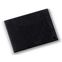
AM29F160DB-70EF Spansion Inc., AM29F160DB-70EF Datasheet - Page 11

AM29F160DB-70EF
Manufacturer Part Number
AM29F160DB-70EF
Description
IC, FLASH, 16MBIT, 70NS, TSOP-48
Manufacturer
Spansion Inc.
Datasheet
1.AM29F160DB-70EF.pdf
(47 pages)
Specifications of AM29F160DB-70EF
Memory Type
Flash
Memory Size
16Mbit
Memory Configuration
2M X 8 / 1M X 16
Ic Interface Type
Parallel
Access Time
70ns
Supply Voltage Range
4.5V To 5.5V
Memory Case Style
TSOP
No. Of Pins
48
Lead Free Status / RoHS Status
Lead free / RoHS Compliant
Available stocks
Company
Part Number
Manufacturer
Quantity
Price
Company:
Part Number:
AM29F160DB-70EF
Manufacturer:
AMD
Quantity:
1
acteristics table represents the active current specifica-
tion for reading array data.
Writing Commands/Command Sequences
To write a command or command sequence (which in-
cludes programming data to the device and erasing
sectors of memory), the system must drive WE# and
CE# to V
An erase operation can erase one sector, multiple sec-
tors, or the entire device. The Sector Address Tables in-
dicate the address space that each sector occupies. A
“sector address” consists of the address bits required
to uniquely select a sector. See the
tions‚ on page 18
or the entire chip, or suspending/resuming the erase
operation.
After the system writes the autoselect command se-
quence, the device enters the autoselect mode. The
system can then read autoselect codes from the inter-
nal register (which is separate from the memory array)
on DQ7–DQ0. Standard read cycle timings apply in this
mode. Refer to the
for more information.
I
tive current specification for the write mode. The “AC
Characteristics” section contains timing specification
tables and timing diagrams for write operations.
Program and Erase Operation Status
During an erase or program operation, the system may
check the status of the operation by reading the status
bits on DQ7–DQ0. Standard read cycle timings and I
read specifications apply. Refer to
Status‚ on page 23
AC Characteristics section for timing diagrams.
Standby Mode
When the system is not reading or writing to the device,
it can place the device in the standby mode. In this
mode, current consumption is greatly reduced, and the
outputs are placed in the high impedance state, inde-
pendent of the OE# input.
The device enters the CMOS standby mode when the
CE# and RESET# are held at V
this is a more restricted voltage range than V
must also either be held at V
The device enters the TTL standby mode when CE#
and RESET# pins are both held at V
quires standard access time (t
the device is in either of these standby modes, before it
is ready to read data.
April 23, 2010 Am29F160D_00_D10
Autoselect Command Sequence‚ on page 19
CC2
in the DC Characteristics table represents the ac-
IL
, and OE# to V
section for details on erasing a sector
Autoselect Mode‚ on page 12
for more information, and to each
IH
.
CC
CE
) for read access when
± 0.5 V or left floating.
CC
± 0.5 V. (Note that
Command Defini-
IH
Write Operation
. The device re-
IH
sections
.) WP#
D A T A S H E E T
Am29F160D
and
CC
The device also enters the standby mode when the RE-
SET# pin is driven low. Refer to the next section,
If the device is deselected during erasure or program-
ming, the device draws active current until the
operation is completed.
In the DC Characteristics tables, I
standby current specification.
Automatic Sleep Mode
The automatic sleep mode minimizes flash device
energy consumption. The device automatically enables
this mode when addresses remain stable for t
ns. The automatic sleep mode is independent of the
CE#, WE#, and OE# control signals. Standard address
access timings provide new data when addresses are
changed. While in sleep mode, output data is latched
and always available to the system.
RESET#: Hardware Reset Pin
The RESET# pin provides a hardware method of reset-
ting the device to reading array data. When the system
drives the RESET# pin low for at least a period of t
the device immediately terminates any operation in
progress, tristates all data output pins, and ignores all
read/write attempts for the duration of the RESET#
pulse. The device also resets the internal state ma-
chine to reading array data. The operation that was in-
terrupted should be reinitiated once the device is ready
to accept another command sequence, to ensure data
integrity. Current is reduced for the duration of the RE-
SET# pulse.
The RESET# pin may be tied to the system reset cir-
cuitry. A system reset would thus also reset the Flash
memory, enabling the system to read the boot-up firm-
ware from the Flash memory.
If RESET# is asserted during a program or erase oper-
ation, the RY/BY# pin remains a “0” (busy) until the in-
ternal reset operation is complete, which requires a
time of t
system can thus monitor RY/BY# to determine whether
the reset operation is complete. If RESET# is asserted
when a program or erase operation is not executing
(RY/BY# pin is “1”), the reset operation is completed
within a time of t
rithms). The system can read data t
SET# pin returns to V
Refer to the AC Characteristics tables for RESET# pa-
rameters and timing diagram.
Output Disable Mode
When the OE# input is at V
disabled. The output pins are placed in the high imped-
ance state.
RESET#: Hardware Reset Pin‚ on page
READY
(during Embedded Algorithms). The
READY
IH
.
(not during Embedded Algo-
IH
, output from the device is
CC3
RH
represents the
9.
after the RE-
ACC
+ 30
RP
9
,


