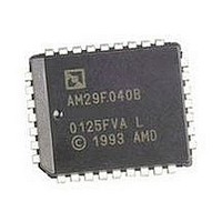
AM29F040B-90JF Spansion Inc., AM29F040B-90JF Datasheet - Page 18

AM29F040B-90JF
Manufacturer Part Number
AM29F040B-90JF
Description
IC, FLASH, 4MBIT, 90NS, LCC-32
Manufacturer
Spansion Inc.
Specifications of AM29F040B-90JF
Memory Type
Flash
Memory Size
4Mbit
Memory Configuration
512K X 8
Access Time
90ns
Supply Voltage Range
4.5V To 5.5V
Memory Case Style
PLCC
No. Of Pins
32
Cell Type
NOR
Density
4Mb
Access Time (max)
90ns
Interface Type
Parallel
Boot Type
Not Required
Address Bus
19b
Operating Supply Voltage (typ)
5V
Operating Temp Range
-40C to 85C
Package Type
PLCC
Program/erase Volt (typ)
4.5 to 5.5V
Sync/async
Asynchronous
Operating Temperature Classification
Industrial
Operating Supply Voltage (min)
4.5V
Operating Supply Voltage (max)
5.5V
Word Size
8b
Number Of Words
512K
Supply Current
30mA
Mounting
Surface Mount
Pin Count
32
Lead Free Status / RoHS Status
Lead free / RoHS Compliant
The DQ5 failure condition may appear if the system
tries to program a “1” to a location that is previously pro-
grammed to “0.” Only an erase operation can change
a “0” back to a “1.” Under this condition, the device
halts the operation, and when the operation has ex-
ceeded the timing limits, DQ5 produces a “1.”
Under both these conditions, the system must issue the
reset command to return the device to reading array
data.
DQ3: Sector Erase Timer
After writing a sector erase command sequence, the
system may read DQ3 to determine whether or not an
erase operation has begun. (The sector erase timer
does not apply to the chip erase command.) If addi-
tional sectors are selected for erasure, the entire time-
out also applies after each additional sector erase com-
mand. When the time-out is complete, DQ3 switches
from “0” to “1.” The system may ignore DQ3 if the sys-
tem can guarantee that the time between additional
sector erase commands is always less than 50 µs. See
also the
After the sector erase command sequence is written,
the system should read the status on DQ7 (Data# Poll-
ing) or DQ6 (Toggle Bit I) to ensure the device has
accepted the command sequence, and then read DQ3.
If DQ3 is “1”, the internally controlled erase cycle has
begun; all further commands (other than Erase Sus-
pend) are ignored until the erase operation is complete.
If DQ3 is “0”, the device accepts additional sector erase
commands. To ensure the command has been ac-
cepted, the system software should check the status of
DQ3 prior to and following each subsequent sector
erase command. If DQ3 is high on the second status
check, the last command might not have been ac-
cepted. Table
16
“Sector Erase Command Sequence”
5
shows the outputs for DQ3.
D A T A
section.
Am29F040B
S H E E T
Notes:
1. Read toggle bit twice to determine whether or not it is
2. Recheck toggle bit because it may stop toggling as DQ5
toggling. See text.
changes to “1”. See text.
No
Figure 4. Toggle Bit Algorithm
Complete, Write
Reset Command
Read DQ7–DQ0
Read DQ7–DQ0
Read DQ7–DQ0
Program/Erase
Operation Not
Toggle Bit
Toggle Bit
= Toggle?
DQ5 = 1?
= Toggle?
START
Twice
Yes
Yes
Yes
21445E8 November 11, 2009
(Notes 1,
2)
(Note
Operation Complete
No
No
Program/Erase
1)


