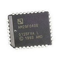
AM29F010B-70JF Spansion Inc., AM29F010B-70JF Datasheet - Page 11

AM29F010B-70JF
Manufacturer Part Number
AM29F010B-70JF
Description
IC, FLASH, 1MBIT, 70NS, LCC-32
Manufacturer
Spansion Inc.
Specifications of AM29F010B-70JF
Memory Type
Flash
Memory Size
1Mbit
Memory Configuration
128K X 8
Access Time
70ns
Supply Voltage Range
4.5V To 5.5V
Memory Case Style
PLCC
No. Of Pins
32
Cell Type
NOR
Density
1Mb
Access Time (max)
70ns
Interface Type
Parallel
Boot Type
Not Required
Address Bus
17b
Operating Supply Voltage (typ)
5V
Operating Temp Range
-40C to 85C
Package Type
PLCC
Program/erase Volt (typ)
4.5 to 5.5V
Sync/async
Asynchronous
Operating Temperature Classification
Industrial
Operating Supply Voltage (min)
4.5V
Operating Supply Voltage (max)
5.5V
Word Size
8b
Number Of Words
128K
Supply Current
30mA
Mounting
Surface Mount
Pin Count
32
Lead Free Status / RoHS Status
Lead free / RoHS Compliant
Available stocks
Company
Part Number
Manufacturer
Quantity
Price
Company:
Part Number:
AM29F010B-70JF
Manufacturer:
NXP
Quantity:
1 560
Company:
Part Number:
AM29F010B-70JF
Manufacturer:
AMD
Quantity:
610
Part Number:
AM29F010B-70JF
Manufacturer:
AMD
Quantity:
20 000
L = Logic Low = V
Sector Protection/Unprotection
The hardware sector protection feature disables both
program and erase operations in any sector. The hard-
ware sector unprotection feature re-enables both
program and erase operations in previously protected
sectors.
Sector protection/unprotection must be implemented
using programming equipment. The procedure re-
quires a high voltage (V
control pins. Details on this method are provided in a
supplement, publication number 22337. Contact an
AMD representative to obtain a copy of the appropriate
document.
The device is shipped with all sectors unprotected.
AMD offers the option of programming and protecting
sectors at its factory prior to shipping the device
through AMD’s ExpressFlash™ Service. Contact an
AMD representative for details.
It is possible to determine whether a sector is protected
or unprotected. See “Autoselect Mode” for details.
Hardware Data Protection
The command sequence requirement of unlock cycles
for programming or erasing provides data protection
against inadvertent writes (refer to the Command Defi-
nitions table). In addition, the following hardware data
protection measures prevent accidental erasure or pro-
November 12, 2009 Am29F010B_00_C10
Manufacturer ID: AMD
Device ID: Am29F010B
Sector Protection Verification
Description
IL
, H = Logic High = V
Table 3. Am29F010B Autoselect Codes (High Voltage Method)
ID
) on address pin A9 and the
CE#
L
L
L
IH
, SA = Sector Address, X = Don’t care.
OE#
L
L
L
D A T A
WE#
H
H
H
A16
A14
SA
to
X
X
S H E E T
A13
A10
to
X
X
X
gramming, which might otherwise be caused by
spurious system level signals during V
power-down transitions, or from system noise.
Low V
When V
cept any write cycles. This protects data during V
power-up and power-down. The command register and
all internal program/erase circuits are disabled, and the
device resets. Subsequent writes are ignored until V
is greater than V
proper signals to the control pins to prevent uninten-
tional writes when V
Write Pulse “Glitch” Protection
Noise pulses of less than 5 ns (typical) on OE#, CE# or
WE# do not initiate a write cycle.
Logical Inhibit
Write cycles are inhibited by holding any one of OE# =
V
CE# and WE# must be a logical zero while OE# is a
logical one.
Power-Up Write Inhibit
If WE# = CE# = V
device does not accept commands on the rising edge
of WE#. The internal state machine is automatically
reset to reading array data on power-up.
IL
, CE# = V
V
V
V
A9
ID
ID
ID
CC
CC
Write Inhibit
A8
A7
is less than V
to
X
X
X
IH
or WE# = V
IL
A6
LKO
L
L
L
and OE# = V
CC
. The system must provide the
is greater than V
A5
A2
to
X
X
X
LKO
IH
, the device does not ac-
. To initiate a write cycle,
A1
H
L
L
IH
during power up, the
A0
H
L
L
CC
LKO
power-up and
(unprotected)
(protected)
.
DQ7
DQ0
01h
20h
01h
00h
to
CC
CC
9


