74HCT08D NXP Semiconductors, 74HCT08D Datasheet - Page 5
74HCT08D
Manufacturer Part Number
74HCT08D
Description
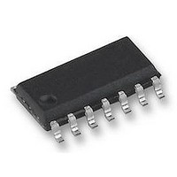
74HCT CMOS, SMD, 74HCT08, SOIC14
Manufacturer
NXP Semiconductors
Datasheet
1.74HCT08D.pdf
(20 pages)
Specifications of 74HCT08D
Output Current
4mA
No. Of Inputs
2
Supply Voltage Range
4.5V To 5.5V
Logic Case Style
SOIC
No. Of Pins
14
Operating Temperature Range
-40°C To +125°C
Svhc
No SVHC
Logic Type
AND Gate
Lead Free Status / RoHS Status
Lead free / RoHS Compliant
Available stocks
Company
Part Number
Manufacturer
Quantity
Price
Company:

Part Number:
74HCT08D
Manufacturer:
PHILIPS
Quantity:
5 750
Part Number:
74HCT08D
Manufacturer:
PHILIPS/飞利浦
Quantity:
20 000
Part Number:
74HCT08D,653
Manufacturer:
NXP/恩智浦
Quantity:
20 000
Part Number:
74HCT08D-T
Manufacturer:
PHILIPS/飞利浦
Quantity:
20 000
Company:
Part Number:
74HCT08D/G
Manufacturer:
PHI
Quantity:
50 000
Company:
Part Number:
74HCT08DR2G
Manufacturer:
ON Semiconductor
Quantity:
61
Company:
Part Number:
74HCT08DTR2G
Manufacturer:
ON Semiconductor
Quantity:
8 000


Philips Semiconductors
RECOMMENDED OPERATING CONDITIONS
LIMITING VALUES
In accordance with the Absolute Maximum Rating System (IEC 60134); voltages are referenced to GND (ground = 0 V).
Notes
1. For DIP14 packages: above 70 C derate linearly with 12 mW/K.
2. For SO14 packages: above 70 C derate linearly with 8 mW/K.
2003 Jul 25
handbook, halfpage
V
V
V
T
t
V
I
I
I
I
T
P
SYMBOL
SYMBOL
r
IK
OK
O
CC
, t
amb
stg
CC
I
O
CC
tot
Quad 2-input AND gate
f
, I
For SSOP14 and TSSOP14 packages: above 60 C derate linearly with 5.5 mW/K.
For DHVQFN14 packages: above 60 C derate linearly with 4.5 mW/K.
GND
A
B
Fig.5 HC logic diagram (one gate).
supply voltage
input voltage
output voltage
ambient
temperature
input rise and fall
times
supply voltage
input diode current
output diode current
output source or sink current
V
storage temperature
power dissipation
CC
PARAMETER
DIP14 package
other packages
or GND current
PARAMETER
see DC and AC
characteristics per device
V
V
V
CC
CC
CC
= 2.0 V
= 4.5 V
= 6.0 V
CONDITIONS
MNB037
Y
V
V
T
T
0.5 V < V
amb
amb
I
O
< 0.5 V or V
< 0.5 V or V
= 40 to +125 C; note 1
= 40 to +125 C; note 2
5
O
CONDITIONS
2.0
0
0
< V
MIN.
40
handbook, halfpage
I
CC
O
> V
> V
+ 0.5 V
74HC08
5.0
+25
6.0
CC
TYP.
CC
A
B
Fig.6 HCT logic diagram (one gate).
+ 0.5 V
+ 0.5 V
6.0
V
V
+125
1000
500
400
MAX.
CC
CC
4.5
0
0
MIN.
40
0.5
65
74HC08; 74HCT08
MIN.
74HCT08
5.0
+25
6.0
TYP.
+7.0
+150
750
500
Product specification
20
20
25
50
MAX.
MNA221
5.5
V
V
+125
500
MAX.
CC
CC
Y
V
mA
mA
mA
mA
mW
mW
C
UNIT
V
V
V
ns
ns
ns
UNIT
C
Related parts for 74HCT08D
Image
Part Number
Description
Manufacturer
Datasheet
Request
R

Part Number:
Description:
IC PARITY GEN/CHKER 9BIT 14SOIC
Manufacturer:
NXP Semiconductors
Datasheet:

Part Number:
Description:
IC MUX/DEMUX 8X1 16SSOP
Manufacturer:
NXP Semiconductors
Datasheet:

Part Number:
Description:
IC MUX/DEMUX 1X16 24TSSOP
Manufacturer:
NXP Semiconductors
Datasheet:

Part Number:
Description:
IC SWITCH SPST UMT5
Manufacturer:
NXP Semiconductors
Datasheet:

Part Number:
Description:
IC SWITCH SPST SC74A
Manufacturer:
NXP Semiconductors
Datasheet:

Part Number:
Description:
IC MUX/DEMUX TRIPLE 2X1 16TSSOP
Manufacturer:
NXP Semiconductors
Datasheet:

Part Number:
Description:
IC MUX/DEMUX 8X1 16SOIC
Manufacturer:
NXP Semiconductors
Datasheet:
Part Number:
Description:
IC SWITCH QUAD 1X1 16SOIC
Manufacturer:
NXP Semiconductors
Datasheet:

Part Number:
Description:
IC SWITCH QUAD 1X2 14TSSOP
Manufacturer:
NXP Semiconductors
Datasheet:

Part Number:
Description:
IC MUX/DEMUX TRIPLE 2X1 16DIP
Manufacturer:
NXP Semiconductors
Datasheet:
Part Number:
Description:
IC SWITCH QUAD 1X1 16DIP
Manufacturer:
NXP Semiconductors
Datasheet:

Part Number:
Description:
IC MUX/DEMUX TRIPLE 2X1 16DHVQFN
Manufacturer:
NXP Semiconductors
Datasheet:
Part Number:
Description:
IC MUX/DEMUX TRIPLE 2X1 16SOIC
Manufacturer:
NXP Semiconductors
Datasheet:

Part Number:
Description:
IC MUX/DEMUX 1X16 24SSOP
Manufacturer:
NXP Semiconductors
Datasheet:

Part Number:
Description:
IC BUFF/DVR TRI-ST 8BIT 20TSSOP
Manufacturer:
NXP Semiconductors
Datasheet: