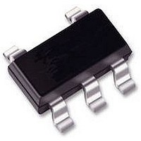
74LVC1G04GW NXP Semiconductors, 74LVC1G04GW Datasheet - Page 4

74LVC1G04GW
Manufacturer Part Number
74LVC1G04GW
Description
IC, INVERTER, 1I/P, SOT-353-5
Manufacturer
NXP Semiconductors
Datasheets
1.74LVC1G04GF.pdf
(15 pages)
2.74LVC1G04GW.pdf
(16 pages)
3.74LVC1G04GW.pdf
(15 pages)
4.74LVC1G04GW.pdf
(15 pages)
Specifications of 74LVC1G04GW
Output Current
32mA
No. Of Inputs
1
Supply Voltage Range
1.65V To 5.5V
Logic Case Style
SOT-353
No. Of Pins
5
Operating Temperature Range
-40°C To +125°C
Logic Type
Inverter Gate
Lead Free Status / RoHS Status
Lead free / RoHS Compliant
Available stocks
Company
Part Number
Manufacturer
Quantity
Price
Company:
Part Number:
74LVC1G04GW
Manufacturer:
NXP
Quantity:
66 000
Part Number:
74LVC1G04GW
Manufacturer:
NXP/恩智浦
Quantity:
20 000
Company:
Part Number:
74LVC1G04GW,125
Manufacturer:
NXP Semiconductors
Quantity:
9 250
Company:
Part Number:
74LVC1G04GWЈ¬125
Manufacturer:
NXP
Quantity:
15 000
Philips Semiconductors
RECOMMENDED OPERATING CONDITIONS
LIMITING VALUES
In accordance with the Absolute Maximum Rating System (IEC 60134); voltages are referenced to GND (ground = 0 V).
Notes
1. The input and output voltage ratings may be exceeded if the input and output current ratings are observed.
2. When V
2002 Oct 02
handbook, halfpage
V
V
V
T
t
V
I
V
I
V
I
I
T
P
r
IK
OK
O
CC
SYMBOL
SYMBOL
, t
amb
stg
CC
I
O
CC
I
O
D
Single inverter
f
, I
GND
CC
supply voltage
input voltage
output voltage
operating ambient temperature
input rise and fall times
supply voltage
input diode current
input voltage
output diode current
output voltage
output source or sink current
V
storage temperature
power dissipation per package
Fig.3 IEE/IEC logic symbol.
= 0 V (Power-down mode), the output voltage can be 5.5 V in normal operation.
CC
2
or GND current
PARAMETER
PARAMETER
1
MNA109
4
active mode
V
V
V
V
note 1
V
active mode; notes 1 and 2
Power-down mode; notes 1 and 2
V
for temperature range from
40 to +125 C
CC
CC
CC
I
O
O
< 0
> V
= 0 to V
= 0 V; Power-down mode
= 1.65 to 2.7 V
= 2.7 to 5.5 V
CC
CONDITIONS
CONDITIONS
or V
4
CC
handbook, halfpage
O
< 0
A
Fig.4 Logic diagram.
1.65
0
0
0
0
0
40
0.5
0.5
0.5
0.5
65
MIN.
MIN.
5.5
5.5
V
5.5
+125
20
10
+6.5
+6.5
V
+6.5
+150
250
MNA110
50
50
50
100
CC
CC
Product specification
74LVC1G04
MAX.
MAX.
+ 0.5 V
Y
V
V
V
V
ns/V
ns/V
V
mA
V
mA
V
mA
mA
mW
C
C
UNIT
UNIT


