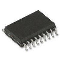
IDT74FCT244ATSOG INTEGRATED DEVICE TECHNOLOGY, IDT74FCT244ATSOG Datasheet - Page 4

IDT74FCT244ATSOG
Manufacturer Part Number
IDT74FCT244ATSOG
Description
LOGIC, FCT, BUFFER/DRIVER, SOIC20
Manufacturer
INTEGRATED DEVICE TECHNOLOGY
Datasheet
1.IDT74FCT244ATSOG8.pdf
(6 pages)
Specifications of IDT74FCT244ATSOG
Supply Voltage Range
4.75V To 5.25V
Logic Case Style
SOIC
No. Of Pins
20
Operating Temperature Range
-40°C To +85°C
Logic Ic Base Number
74244
Logic Ic Family
FCT
Logic Ic
RoHS Compliant
Package / Case
SOIC
Logic Device Type
Buffer / Line Driver, Non Inverting
Rohs Compliant
Yes
POWER SUPPLY CHARACTERISTICS
NOTES:
1. See test circuit and waveforms.
2. Minimum limits are guaranteed but not tested on Propagation Delays.
NOTES:
1. For conditions shown as Min. or Max., use appropriate value specified under Electrical Characteristics for the applicable device type.
2. Typical values are at V
3. Per TTL driven input; (V
4. This parameter is not directly testable, but is derived for use in Total Power Supply Calculations.
5. Values for these conditions are examples of ΔI
6. I
All currents are in milliamps and all frequencies are in megahertz.
SWITCHING CHARACTERISTICS OVER OPERATING RANGE
IDT54/74FCT244T/AT/CT
FAST CMOS OCTAL BUFFER/LINE DRIVER
Symbol
t
t
t
t
t
t
PLH
PHL
PZH
PZL
PHZ
PLZ
Symbol
I
I
ΔI
D
N
I
f
f
N
C
C
CC
CCD
CP
i
H
T
i
ΔI
I
= Output Frequency
CC
= I
CCD
= I
= Number of Outputs at f
I
= Number of TTL Inputs at D
= Duty Cycle for TTL Inputs High
C
= Quiescent Current
= Clock Frequency for Register Devices (Zero for Non-Register Devices)
CC
QUIESCENT
CC
= Dynamic Current caused by an Input Transition Pair (HLH or LHL)
= Power Supply Current for a TTL High Input (V
+ ΔI
Propagation Delay
Dx to Ox
Output Enable Time
Output Disable Time
CC
Quiescent Power Supply Current
TTL Inputs HIGH
Dynamic Power Supply
Current
Total Power Supply Current
+ I
D
Parameter
H
INPUTS
N
T
+ I
(4)
CC
+ I
IN
CCD
= 3.4V). All other inputs at V
DYNAMIC
= 5.0V, +25°C ambient.
Parameter
i
(f
CP
H
/2+ f
i
N
i
)
(6)
CC
formula. These limits are guaranteed but not tested.
IN
Condition
R
C
CC
= 3.4V)
L
L
= 500Ω
V
V
V
Outputs Open
OE
One Input Toggling
50% Duty Cycle
V
Outputs Open
fi = 10MHz
50% Duty Cycle
OE
One Bit Toggling
V
Outputs Open
fi = 2.5MHz
50% Duty Cycle
OE
Eight Bits Toggling
= 50pF
or GND.
CC
IN
CC
CC
CC
A
A
A
= 3.4V
= Max.
= Max.
= Max.
= Max.
= OE
= OE
= OE
(1)
(3)
B
B
B
Min.
= GND
= GND
= GND
1.5
1.5
1.5
54FCT244T
(2)
Mil.
Test Conditions
Max.
8.5
7.5
7
4
Min.
1.5
1.5
1.5
V
V
V
V
V
V
V
V
V
V
(2)
Ind.
(1)
IN
IN
IN
IN
IN
IN
IN
IN
IN
IN
54/74FCT244AT
= V
= V
= V
= GND
= GND
= 3.4V
= GND
= GND
= 3.4V
= GND
Max.
4.8
6.2
5.6
MILITARY AND INDUSTRIAL TEMPERATURE RANGES
CC
CC
CC
Min.
1.5
1.5
1.5
(2)
Mil.
Max.
5.1
6.5
5.9
Min.
—
—
—
—
—
—
Min.
1.5
1.5
1.5
(2)
Ind.
54/74FCT244CT
Typ.
Max.
0.15
0.5
1.5
1.8
4.1
5.8
5.2
3
5
(2)
Min.
1.5
1.5
1.5
Max.
0.25
14
3.5
4.5
6
2
(5)
(2)
(5)
Mil.
Max.
4.6
6.5
5.7
MHz
Unit
mA/
mA
mA
Unit
ns
ns
ns


