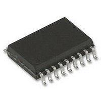
74ABT245D NXP Semiconductors, 74ABT245D Datasheet - Page 2

74ABT245D
Manufacturer Part Number
74ABT245D
Description
74ABT BUS INTERFACE, SMD, 74ABT245
Manufacturer
NXP Semiconductors
Datasheet
1.74ABT245D.pdf
(9 pages)
Specifications of 74ABT245D
Logic Device Type
Transceiver, Non Inverting
Supply Voltage Range
4.5V To 5.5V
Logic Case Style
SOIC
No. Of Pins
20
Operating Temperature Range
-40°C To +85°C
Svhc
No SVHC (18-Jun-2010)
Lead Free Status / RoHS Status
Lead free / RoHS Compliant
Available stocks
Company
Part Number
Manufacturer
Quantity
Price
Part Number:
74ABT245D
Manufacturer:
NXP/恩智浦
Quantity:
20 000
Company:
Part Number:
74ABT245DB
Manufacturer:
PHILIPS
Quantity:
17 617
Part Number:
74ABT245DB
Manufacturer:
PHILIPS/飞利浦
Quantity:
20 000
Philips Semiconductors
FEATURES
QUICK REFERENCE DATA
ORDERING INFORMATION
PIN CONFIGURATION
20-Pin plastic SO
20-Pin Plastic SSOP Type II
20-Pin Plastic TSSOP Type I
2003 Feb 06
Octal bidirectional bus interface
3-State buffers
Output capability: +64 mA/–32 mA
Latch-up protection exceeds 500 mA per Jedec Std 17
ESD protection exceeds 2000 V per MIL STD 833 Method 3015
and 200 V per Machine Model
Power-up 3-State
Live insertion/extraction permitted
Inputs are disabled during 3-State mode
Octal transceiver with direction pin (3-State)
SYMBOL
I
t
t
C
C
PLH
PHL
CCZ
I/O
IN
PACKAGES
Propagation delay
An to Bn or Bn to An
Input capacitance DIR, OE
I/O pin capacitance
Total supply current
GND
DIR
A0
A1
A2
A3
A4
A5
A6
A7
10
1
2
3
4
5
6
7
8
9
PARAMETER
SA00121
20
19
18
17
16
15
14
13
12
11
V
OE
B0
B1
B2
B3
B4
B5
B6
B7
CC
TEMPERATURE RANGE
–40 C to +85 C
–40 C to +85 C
–40 C to +85 C
C
V
Outputs disabled; V
Outputs disabled; V
I
L
= 0 V or V
= 50 pF; V
T
2
CC
amb
CC
DESCRIPTION
The 74ABT245 high-performance BiCMOS device combines low
static and dynamic power dissipation with high speed and high
output drive.
The 74ABT245 device is an octal transceiver featuring non-inverting
3-State bus compatible outputs in both send and receive directions.
The control function implementation minimizes external timing
requirements. The device features an Output Enable (OE) input for
easy cascading and a Direction (DIR) input for direction control.
PIN DESCRIPTION
= 5 V
CONDITIONS
= 25 C; GND = 0 V
18, 17, 16,
15, 14, 13,
NUMBER
2, 3, 4, 5,
6, 7, 8, 9
O
CC
12, 11
PIN
= 0 V or V
19
10
20
1
=5.5 V
CC
PART NUMBER
SYMBOL
A0 – A7
B0 – B7
74ABT245PW
74ABT245DB
74ABT245D
GND
V
DIR
OE
CC
Direction control input
Data inputs/outputs (A side)
Data inputs/outputs (B side)
Output enable input (active-LOW)
Ground (0 V)
Positive supply voltage
NAME AND FUNCTION
TYPICAL
2.2
2.9
50
4
7
74ABT245
DWG NUMBER
SOT163-1
SOT339-1
SOT360-1
Product data
UNIT
pF
pF
ns
A


