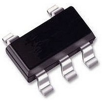
74LVC1G126GW NXP Semiconductors, 74LVC1G126GW Datasheet - Page 2

74LVC1G126GW
Manufacturer Part Number
74LVC1G126GW
Description
IC, LOGIC, 74LVC1G, BUFFER, UMT5
Manufacturer
NXP Semiconductors
Datasheet
1.74LVC1G126GW.pdf
(19 pages)
Specifications of 74LVC1G126GW
Supply Voltage Range
1.65V To 5.5V
Logic Case Style
SOT-353
No. Of Pins
5
Operating Temperature Range
-40°C To +125°C
Svhc
No SVHC (18-Jun-2010)
Logic Ic Base
RoHS Compliant
Package / Case
SOT-353
Logic Device Type
Buffer / Line Driver, Non Inverting
Rohs Compliant
Yes
Available stocks
Company
Part Number
Manufacturer
Quantity
Price
Part Number:
74LVC1G126GW
Manufacturer:
NXP/恩智浦
Quantity:
20 000
Company:
Part Number:
74LVC1G126GW,125
Manufacturer:
NXP Semiconductors
Quantity:
4 750
Part Number:
74LVC1G126GW,125
Manufacturer:
NEXPERIA/安世
Quantity:
20 000
Company:
Part Number:
74LVC1G126GWЈ¬125
Manufacturer:
NXP
Quantity:
3 000
NXP Semiconductors
3. Ordering information
Table 1.
4. Marking
Table 2.
[1]
5. Functional diagram
74LVC1G126
Product data sheet
Type number
74LVC1G126GW
74LVC1G126GV
74LVC1G126GM
74LVC1G126GF
74LVC1G126GN
Type number
74LVC1G126GW
74LVC1G126GV
74LVC1G126GM
74LVC1G126GF
74LVC1G126GN
74LVC1G126GS
74LVC1G126GS
Fig 1.
The pin 1 indicator is located on the lower left corner of the device, below the marking code.
2
1
Logic symbol
Ordering information
Marking codes
A
OE
mna125
Package
Temperature range
40 C to +125 C
40 C to +125 C
40 C to +125 C
40 C to +125 C
40 C to +125 C
40 C to +125 C
Y
4
All information provided in this document is subject to legal disclaimers.
Fig 2.
Rev. 10 — 29 December 2010
Name
TSSOP5
SC-74A
XSON6
XSON6
XSON6
XSON6
2
1
IEC logic symbol
OE
Marking
VN
V26
VN
VN
VN
VN
mna126
plastic extremely thin small outline package;
plastic extremely thin small outline package;
extremely thin small outline package; no leads;
Description
plastic thin shrink small outline package;
5 leads; body width 1.25 mm
plastic surface-mounted package; 5 leads
no leads; 6 terminals; body 1 1.45 0.5 mm
no leads; 6 terminals; body 1 1 0.5 mm
6 terminals; body 0.9 1.0 0.35 mm
extremely thin small outline package; no leads;
6 terminals; body 1.0 1.0 0.35 mm
[1]
4
Fig 3.
OE
A
Bus buffer/line driver; 3-state
Logic diagram
74LVC1G126
© NXP B.V. 2010. All rights reserved.
Version
SOT353-1
SOT753
SOT886
SOT891
SOT1115
SOT1202
mna127
2 of 19
Y


