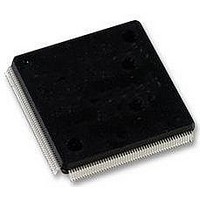
LFXP6C-5QN208C LATTICE SEMICONDUCTOR, LFXP6C-5QN208C Datasheet - Page 32

LFXP6C-5QN208C
Manufacturer Part Number
LFXP6C-5QN208C
Description
FPGA, 1.8V FLASH, INSTANT ON, SMD
Manufacturer
LATTICE SEMICONDUCTOR
Series
LatticeXPr
Datasheet
1.LFXP3C-3QN208C.pdf
(130 pages)
Specifications of LFXP6C-5QN208C
No. Of Logic Blocks
720
No. Of Macrocells
3000
Family Type
LatticeXP
No. Of Speed Grades
5
No. Of I/o's
142
Clock Management
PLL
Core Supply Voltage Range
1.71V To 3.465V
Lead Free Status / RoHS Status
Lead free / RoHS Compliant
Available stocks
Company
Part Number
Manufacturer
Quantity
Price
Company:
Part Number:
LFXP6C-5QN208C
Manufacturer:
Lattice Semiconductor Corporation
Quantity:
10 000
www.latticesemi.com
© 2007 Lattice Semiconductor Corp. All Lattice trademarks, registered trademarks, patents, and disclaimers are as listed at www.latticesemi.com/legal. All other brand
or product names are trademarks or registered trademarks of their respective holders. The specifications and information herein are subject to change without notice.
Absolute Maximum Ratings
1. Stress above those listed under the “Absolute Maximum Ratings” may cause permanent damage to the device. Functional operation of the
2. Compliance with the Lattice Thermal Management document is required.
3. All voltages referenced to GND.
4. All chip grounds are connected together to a common package GND plane.
5. Overshoot and undershoot of -2V to (V
November 2007
Recommended Operating Conditions
Supply Voltage V
Supply Voltage V
Supply Voltage V
Supply Voltage V
Output Supply Voltage V
I/O Tristate Voltage Applied
Dedicated Input Voltage Applied
Storage Temperature (Ambient) . . . . . . . . . . . . . . -65 to 150°C . . . . . . . . . . . . . . . -65 to 150°C
Junction Temp. (Tj) . . . . . . . . . . . . . . . . . . . . . . . . . . +125°C . . . . . . . . . . . . . . . . . . . +125°C
V
V
V
V
V
t
t
t
t
1. If V
2. See recommended voltages by I/O standard in subsequent table.
3. The system designer must ensure that the FPGA design stays within the specified junction temperature and package thermal capabilities of
4. V
JCOM
JIND
JFLASHCOM
JFLASHIND
CC
CCP
CCAUX
CCIO
CCJ
device at these or any other conditions outside of those indicated in the operational sections of this specification is not implied.
Symbol
V
the device based on the expected operating frequency, activity factor and environment conditions of the system.
CCJ
CCAUX
1
CCIO
1, 2
4
is set to 1.2V, they must be connected to the same power supply as V
or V
ramp rate must not exceed 30mV/µs during power up when transitioning between 0V and 3.3V.
CCJ
Core Supply Voltage for 1.2V Devices
Core Supply Voltage for 1.8V/2.5V/3.3V Devices
Supply Voltage for PLL for 1.2V Devices
Supply Voltage for PLL for 1.8V/2.5V/3.3V Devices
Auxiliary Supply Voltage
I/O Driver Supply Voltage
Supply Voltage for IEEE 1149.1 Test Access Port
Junction Temperature, Commercial Operation
Junction Temperature, Industrial Operation
Junction Temperature, Flash Programming, Commercial
Junction Temperature, Flash Programming, Industrial
is set to 3.3V, they must be connected to the same power supply as V
CC
CCP
CCAUX
CCJ
. . . . . . . . . . . . . . . . . . . . . . . . -0.5 to 1.32V . . . . . . . . . . . . . . . -0.5 to 3.75V
. . . . . . . . . . . . . . . . . . . . . . . -0.5 to 1.32V . . . . . . . . . . . . . . . -0.5 to 3.75V
. . . . . . . . . . . . . . . . . . . . . . . -0.5 to 3.75V . . . . . . . . . . . . . . . -0.5 to 3.75V
. . . . . . . . . . . . . . . . . . . . . -0.5 to 3.75V . . . . . . . . . . . . . . . -0.5 to 3.75V
CCIO
5
. . . . . . . . . . . . . . . . . -0.5 to 3.75V . . . . . . . . . . . . . . . -0.5 to 3.75V
. . . . . . . . . . . . . . . . -0.5 to 3.75V . . . . . . . . . . . . . . . -0.5 to 3.75V
5
IHMAX
. . . . . . . . . . . . . -0.5 to 3.75V . . . . . . . . . . . . . . . -0.5 to 4.25V
+ 2) volts is permitted for a duration of <20ns.
1, 2, 3, 4
DC and Switching Characteristics
Parameter
XPE (1.2V)
LatticeXP Family Data Sheet
3-1
3
CC
.
CCAUX.
For the XPE devices (1.2V V
XPC (1.8V/2.5V/3.3V)
DS1001
3.135
Min.
1.14
1.71
1.14
1.71
1.14
1.14
-40
0
0
0
DC and Switching_02.7
Data Sheet DS1001
3.465
3.465
3.465
3.465
3.465
Max.
1.26
1.26
100
85
85
85
CC
), if V
Units
CCIO
V
V
V
C
C
C
C
V
V
V
V
or


