CLC021AVGZ-3.3 National Semiconductor, CLC021AVGZ-3.3 Datasheet - Page 9
CLC021AVGZ-3.3
Manufacturer Part Number
CLC021AVGZ-3.3
Description
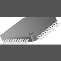
IC, DIG VIDEO SERIALIZER, 3.63V, PQFP-44
Manufacturer
National Semiconductor
Datasheet
1.CLC021AVGZ-3.3.pdf
(18 pages)
Specifications of CLC021AVGZ-3.3
Ic Interface Type
Parallel, Serial
Supply Voltage Range
2.97V To 3.63V
Power Dissipation Pd
235mW
Operating Temperature Range
0°C To +70°C
Digital Ic Case Style
PQFP
No. Of Pins
44
Operating Temperature (min)
0C
Operating Temperature Classification
Commercial
Operating Temperature (max)
70C
Package Type
PQFP
Rad Hardened
No
Lead Free Status / RoHS Status
Contains lead / RoHS non-compliant
Lead Free Status / RoHS Status
Contains lead / RoHS non-compliant
Available stocks
Company
Part Number
Manufacturer
Quantity
Price
Company:

Part Number:
CLC021AVGZ-3.3
Manufacturer:
Texas Instruments
Quantity:
10 000
Part Number:
CLC021AVGZ-3.3
Manufacturer:
TI/德州仪器
Quantity:
20 000
Company:
Part Number:
CLC021AVGZ-3.3/NOPB
Manufacturer:
NSC
Quantity:
96
Company:
Part Number:
CLC021AVGZ-3.3/NOPB
Manufacturer:
Texas Instruments
Quantity:
10 000


Device Operation
NRZ-TO-NRZI CONVERTER
The NRZ-to-NRZI converter accepts NRZ serial data from
the SMPTE and EDH polynomial genertors and converts it to
NRZI using the polynomial (X + 1) per SMPTE 259M, para-
graph 5.2 and Annex C. The converter’s output goes to the
output buffer amplifier. The NRZ/NRZI input enables this
conversion function. Conversion from NRZ to NRZI is en-
abled when the input is a logic LOW. Conversion to NRZI is
disabled when this input is a logic-HIGH. This function is not
affected by the SMPTE mode control input. The input pin is
pulled internally to V
EDH SYSTEM OPERATION
The CLC021 has EDH character and flag generation and
insertion circuitry which operates as proposed in SMPTE
RP-165. Inputs and circuitry are provided to control genera-
tion and automatic insertion of the EDH check words at
proper locations in the serial data output.
The EDH polynomial generators accept parallel data from
the input register and generate 16-bit serial check words
using the polynomial X
tions are made for each video field prior to serialization.
Separate CRCs for the full-field and active picture along with
status flags are inserted and serially transmitted with the
other data. Upon being reset, the initial state of all EDH
check characters is 00h.
The EDH control system accepts input from the sync detec-
tor and controls the EDH polynomial generator and SMPTE/
EDH polynomial insertion multiplexer. EDH Enable, an ex-
ternal TTL-compatible, low-true input, enables this circuitry.
The controller inserts the EDH check words in the serial data
stream at the correct positions in the ancilliary data space
per SMPTE 259M paragraph 7.3, 8.4.4 or 9.4.4 and per
SMPTE RP-165. Ancilliary data space is formatted per
SMPTE 291M.
The EDH Force control input causes the insertion of new
EDH checkwords and flags into the serial output regardless
of the previous condition of EDH checkwords and flags in the
input parallel data. This function may be used in situations
where video content has been editted thus making the pre-
vious EDH information invalid.
The NTSC/PAL output indicates the type of component or
composite data standard being input to the CLC021. This
output is useful for troubleshooting or may be used to drive a
panel indicator. The output is high when 625-line PAL data is
being input and low when 525-line NTSC data is being input.
PHASE-LOCKED LOOP AND VCO
The phase-locked loop (PLL) system generates the output
serial data clock at 10x the parallel data clock frequency.
This system consists of a VCO, divider chain, phase-
frequency detector and internal loop filter. The VCO free-
SS
16
(NRZI enabled) when unconnected.
+ X
12
(Continued)
+ X
6
+ 1. Separate calcula-
9
running frequency is internally set. The PLL automatically
generates the appropriate frequency for the serial clock rate
using the parallel data clock (P
ence. Loop filtering is internal to the CLC021. The VCO halts
when no P
applied after power to the device.
The VCO has separate V
pins 27 and 28, which may be supplied power via an external
low-pass filter, if desired. The PLL acquisition (lock) time is
less than 75 µs
LOCK DETECT
The lock detect output (pin 26) of the phase-frequency de-
tector is a logic HIGH when the loop is locked. The output is
CMOS/TTL-compatible and is suitable for driving other
CMOS devices or an LED indicator. The Lock Detect pin
reports the status of the PLL. When P
low at the event.
SERIAL DATA OUTPUT BUFFER
The current-mode serial data outputs provide low-skew
complimentary or differential signals. The output buffer de-
sign can drive 75Ω coaxial cables (AC-coupled) or 10K/100K
ECL/PECL-compatible devices (DC-coupled). Output levels
are 800 mV
loads. The output level is 400 mV
coupled into 75Ω. (See Application Information for details.)
The 75Ω resistors connected to the SDO outputs are back-
matching resistors. No series back-matching resistors
should be used. Output level is controlled by the value of
R
1.69 kΩ,
in an out-of-lock condition. Separate V
power feeds, pins, 37 and 40 are provided for the serial
output driver.
POWER-ON RESET AND RESET INPUT
The CLC021 has an internally controlled, automatic, power-
on-reset circuit. Reset clears TRS detection circuitry, all
latches, registers, counters and polynomial generators, sets
the EDH characters to 00h and disables the serial output.
The SDO outputs are tri-stated during power-on reset. The
part will remain in the reset condition until the parallel input
clock is applied.
An active-HIGH-true, manual reset input is available at
pin 1. It resets both the digital and PLL blocks. The reset
input has an internal pull-down device and is inactive when
unconnected.
It is recommended that P
30 µs after power has reached V
manual reset is used during power-on, then P
asserted at any time as long as manual reset is not de-
asserted until V
REF
connected to pin 35. The value of R
±
CLK
1%. The output buffer is static when the device is
P-P
signal is present or is inactive. P
DD
±
@
10% into 75Ω AC-coupled, back-matched
min is reached. See Figure 5.
270 Mbps.
SSO
CLK
and V
not be asserted until at least
CLK
DD
DDO
) frequency as its refer-
CLK
P-P
min. See Figure 4. If
power supply feeds,
is lost, it will switch
±
SSSD
10% when DC-
REF
CLK
CLK
and V
www.national.com
is normally
should be
may be
DDSD
Related parts for CLC021AVGZ-3.3
Image
Part Number
Description
Manufacturer
Datasheet
Request
R

Part Number:
Description:
BOARD EVALUATION CLC021AVGZ-3.3
Manufacturer:
National Semiconductor
Datasheet:
Part Number:
Description:
BOARD EVALUATION CLC021AVGZ-5.0
Manufacturer:
National Semiconductor
Datasheet:
Part Number:
Description:
National Semiconductor [8-Bit D/A Converter]
Manufacturer:
National Semiconductor
Datasheet:
Part Number:
Description:
National Semiconductor [Media Coprocessor]
Manufacturer:
National Semiconductor
Datasheet:
Part Number:
Description:
Digitally Controlled Tone and Volume Circuit with Stereo Audio Power Amplifier, Microphone Preamp Stage and National 3D Sound
Manufacturer:
National Semiconductor
Datasheet:
Part Number:
Description:
Digitally Controlled Tone and Volume Circuit with Stereo Audio Power Amplifier, Microphone Preamp Stage and National 3D Sound
Manufacturer:
National Semiconductor
Datasheet:
Part Number:
Description:
AC97 Rev 2 Codec with Sample Rate Conversion and National 3D Sound
Manufacturer:
National Semiconductor
Part Number:
Description:
Manufacturer:
National Semiconductor
Datasheet:
Part Number:
Description:
Manufacturer:
National Semiconductor
Datasheet:
Part Number:
Description:
General Purpose, Low Voltage, Low Power, Rail-to-Rail Output Operational Amplifiers
Manufacturer:
National Semiconductor
Datasheet:
Part Number:
Description:
8-bit 20 MSPS flash A/D converter.
Manufacturer:
National Semiconductor
Datasheet:
Part Number:
Description:
Low Noise Quad Operational Amplifier
Manufacturer:
National Semiconductor
Datasheet:
Part Number:
Description:
Quad Differential Line Receivers
Manufacturer:
National Semiconductor
Datasheet:
Part Number:
Description:
Quad High Speed Trapezoidal? Bus Transceiver
Manufacturer:
National Semiconductor
Datasheet: