ADM3101EACPZ-250R7 Analog Devices Inc, ADM3101EACPZ-250R7 Datasheet - Page 5
ADM3101EACPZ-250R7
Manufacturer Part Number
ADM3101EACPZ-250R7
Description
IC, RS-232 TXRX, 460KBPS, 5.5V, LFCSP-12
Manufacturer
Analog Devices Inc
Type
Transceiverr
Datasheet
1.ADM3101EACPZ-REEL.pdf
(12 pages)
Specifications of ADM3101EACPZ-250R7
Device Type
Transceiver
Ic Interface Type
RS232
No. Of Drivers
1
Supply Voltage Range
3V To 5.5V
Driver Case Style
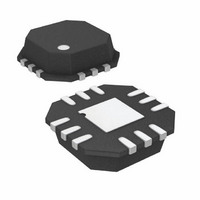
LFCSP
No. Of Pins
12
Operating Temperature Range
-40°C To +85°C
Number Of Drivers/receivers
1/1
Protocol
RS232
Voltage - Supply
3 V ~ 3.6 V
Mounting Type
Surface Mount
Package / Case
12-LFCSP
Data Rate
460Kbps
Number Of Receivers
1
Number Of Transmitters
1
Number Of Transceivers
1
Receiver Signal Type
Single-Ended
Transmitter Signal Type
Single-Ended
Single Supply Voltage (typ)
3.3V
Single Supply Voltage (min)
3V
Single Supply Voltage (max)
5.5V
Dual Supply Voltage (typ)
Not RequiredV
Dual Supply Voltage (min)
Not RequiredV
Dual Supply Voltage (max)
Not RequiredV
Supply Current
5mA
Power Supply Requirement
Single
Operating Temp Range
-40C to 85C
Operating Temperature Classification
Industrial
Mounting
Surface Mount
Pin Count
12
Package Type
LFCSP EP
Lead Free Status / RoHS Status
Lead free / RoHS Compliant
Lead Free Status / RoHS Status
Lead free / RoHS Compliant, Lead free / RoHS Compliant
Other names
ADM3101EACPZ-250R7TR
Available stocks
Company
Part Number
Manufacturer
Quantity
Price
Company:

Part Number:
ADM3101EACPZ-250R7
Manufacturer:
INFINEON
Quantity:
101
Part Number:
ADM3101EACPZ-250R7
Manufacturer:
ADI/亚德诺
Quantity:
20 000


PIN CONFIGURATIONS AND FUNCTION DESCRIPTIONS
Table 3. Pin Function Descriptions
LFCSP
1, 12
2
3
4
5
6
7
8
9
10, 11
N/A
Pin No.
QSOP
2, 1
4
5
7
8
9
10
12
13
15, 16
3, 6, 11, 14
Mnemonic
C1+, C1−
R
T
V+
V
GND
V–
T
R
C2−, C2+
NC
IN
OUT
OUT
CC
IN
Description
Positive and Negative Connections for Charge Pump Capacitor. External Capacitor C1 is connected
between these pins; a 0.1 μF capacitor is recommended, but larger capacitors up to 10 μF can be used.
Receiver Output. This pin outputs CMOS output logic levels.
Transmitter (Driver) Input. This input accepts TTL/CMOS levels.
Internally Generated Positive Supply (+6 V Nominal).
Power Supply Input, 3.0 V to 5.5 V.
Ground. Must be connected to 0 V.
Internally Generated Negative Supply (−6 V Nominal).
Transmitter (Driver) Output. This pin outputs RS-232 signal levels (typically ±6 V).
Receiver Input. This input accepts RS-232 signal levels. An internal 5 kΩ pull-down resistor to GND is
connected on the input.
Positive and Negative Connections for Charge Pump Capacitor. External Capacitor C2 is connected
between these pins; a 0.1 μF capacitor is recommended, but larger capacitors up to 10 μF can be used.
No Connect. These pins should always remain unconnected.
NOTES
1. PADDLE CONNECTED TO GND. THIS CONNECTION IS NOT
REQUIRED TO MEET THE ELECTRICAL PERFORMANCES.
R
R
C1+
OUT
T
Figure 2. LFCSP Pin Configuration
C1–
C1+
V
Figure 3. QSOP Pin Configuration
OUT
NC
T
NC
IN
V+
CC
IN
1
2
3
1
2
3
4
5
6
7
8
NC = NO CONNECT
Rev. C | Page 5 of 12
ADM3101E
ADM3101E
(Not to Scale)
(Not to Scale)
TOP VIEW
TOP VIEW
PIN 1
INDICATOR
16
15
14
13
12
11
10
9
9 R
8 T
7 V–
C2+
C2–
NC
R
T
NC
V–
GND
OUT
IN
OUT
IN
ADM3101E
Related parts for ADM3101EACPZ-250R7
Image
Part Number
Description
Manufacturer
Datasheet
Request
R

Part Number:
Description:
?15 Kv Esd Protected, 3.3 V Single-channel Rs-232 Line Driver/receiver
Manufacturer:
Analog Devices, Inc.
Datasheet:

Part Number:
Description:
±1.7g Dual-Axis IMEMS Accelerometer Evaluation Board
Manufacturer:
Analog Devices Inc
Datasheet:

Part Number:
Description:
Inertial Sensor Evaluation System
Manufacturer:
Analog Devices Inc
Datasheet:
Part Number:
Description:
Manufacturer:
Analog Devices Inc
Datasheet:
Part Number:
Description:
Manufacturer:
Analog Devices Inc
Datasheet:
Part Number:
Description:
Manufacturer:
Analog Devices Inc
Datasheet:
Part Number:
Description:
Manufacturer:
Analog Devices Inc
Datasheet:
Part Number:
Description:
Manufacturer:
Analog Devices Inc
Datasheet:
Part Number:
Description:
Manufacturer:
Analog Devices Inc
Datasheet:
Part Number:
Description:
Manufacturer:
Analog Devices Inc
Datasheet:
Part Number:
Description:
Manufacturer:
Analog Devices Inc
Datasheet:
Part Number:
Description:
Manufacturer:
Analog Devices Inc
Datasheet:
Part Number:
Description:
Manufacturer:
Analog Devices Inc
Datasheet: