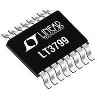
LT3799IMSE#PBF Linear Technology, LT3799IMSE#PBF Datasheet - Page 14

LT3799IMSE#PBF
Manufacturer Part Number
LT3799IMSE#PBF
Description
IC, LED DRVR, MSOP-16
Manufacturer
Linear Technology
Datasheet
1.LT3799EMSEPBF.pdf
(20 pages)
Specifications of LT3799IMSE#PBF
Led Driver Application
High Power LED Driver, Automotive Lighting
No. Of Outputs
1
Output Current
3A
Input Voltage
18V
Dimming Control Type
Analog
Topology
Flyback
Rohs Compliant
Yes
Lead Free Status / RoHS Status
Lead free / RoHS Compliant
Available stocks
Company
Part Number
Manufacturer
Quantity
Price
not solve the problem completely for other supply voltages.
Another systematic error is that the current comparator
cannot instantaneously turn off the main power device.
This delay time leads to primary current overshoot. This
overshoot is less of a problem when the output current is
close to its maximum, since the overshoot is only related
to the slope of the primary current and not the current
level. The overshoot is proportional to the supply voltage,
so again this affects the line regulation.
Universal Input
The LT3799 operates over the universal input range of
90V
be minimized by using two application circuits for the
wide input range: one optimized for 120V
optimized for 220V
the Typical Applications section shows three options:
universal input, 120V
three resistors. In the Typical Performance Characteristics
section, the LED Current vs V
current line regulation for all three circuits.
Selecting Winding Turns Ratio
Boundary mode operation gives a lot of freedom in selecting
the turns ratio of the transformer. We suggest to keep the
duty cycle low, lower N
since the duty cycle will increase when the AC waveform is
decreases to zero volts. A higher N
LT3799
OPERATION
14
AC
to 265V
AC
. Output current regulation error may
AC
AC
. The first application pictured in
, and 220V
PS
, at the maximum input voltage
IN
graphs show the output
AC
PS
. The circuit varies by
increases the output
AC
and another
V
SUPPLY
GATE
Figure 3. Clamp
3799 F03
current while keeping the primary current limit constant.
Although this seems to be a good idea, it comes at the
expense of a higher RMS current for the secondary-side
diode which might not be desirable because of the primary
side MOSFET’s superior performance as a switch. A higher
NPS does reduce the voltage stress on the secondary-side
diode while increasing the voltage stress on the primary-
side MOSFET. If switching frequency at full output load is
kept constant, the amount of energy delivered per cycle by
the transformer also stays constant regardless of the N
Therefore, the size of the transformer remains the same at
practical N
find an optimal MOSFET and diode for a given application.
Switch Voltage Clamp Requirement
Leakage inductance of an offline transformer is high due
to the extra isolation requirement. The leakage inductance
energy is not coupled to the secondary and goes into
the drain node of the MOSFET. This is problematic since
400V and higher rated MOSFETs cannot always handle
this energy by avalanching. Therefore the MOSFET needs
protection. A transient voltage suppressor (TVS) and
diode are recommended for all offline application and
connected, as shown in Figure 3. The TVS device needs
a reverse breakdown voltage greater than (V
where V
V
turns ratio.
f
is the secondary diode forward voltage, and N is the
OUT
PS
is the output voltage of the flyback converter,
’s. Adjusting the turns ratio is a good way to
OUT
+ V
f
)*N
3799f
PS
.


