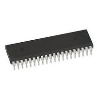
MAX6952EPL+ Maxim Integrated Products, MAX6952EPL+ Datasheet - Page 6

MAX6952EPL+
Manufacturer Part Number
MAX6952EPL+
Description
LED Driver IC
Manufacturer
Maxim Integrated Products
Specifications of MAX6952EPL+
Operating Temperature Range
-40°C To +85°C
Driver Case Style
DIP
Peak Reflow Compatible (260 C)
Yes
Device Type
LED
Display Interface
Common Cathode, Multiplexed
Termination Type
Through Hole
Filter Terminals
Through Hole
Rohs Compliant
Yes
Led Display Type
Dot Matrix / Graphic
Lead Free Status / RoHS Status
Lead free / RoHS Compliant
Figure 1. Functional Diagram
4-Wire Interfaced, 2.7V to 5.5V,
4-Digit 5
Table 1. Connection Scheme for Four Monocolor Digits
Table 2. Connection Scheme for Two Bicolor Digits
Table 3. Serial-Data Format (16 Bits)
6
BLINK
DIGIT O0 O1 O2 O3 O4 O5 O6 O7 O8 O9 O10 O11 O12 O13 O14 O15 O16 O17 O18 O19 O20 O21 O22 O23
DIGIT O0 O1 O2 O3 O4 O5 O6 O7 O8 O9 O10 O11 O12 O13 O14 O15 O16 O17 O18 O19 O20 O21 O22 O23
R/W
DOUT
OSC
ISET
CLK
D15
DIN
1
2
1
2
CS
_______________________________________________________________________________________
Digit 0 rows (cathodes) R1 to R14
Digit 0 rows (cathodes) R1 to R7
Digit 1 rows (cathodes) R1 to R7
COUNTER
NETWORK
ADDRESS
DIVIDER/
D14
CURRENT
SOURCE
SELECT
SPEED
BLINK
D13
RAM
CHARACTER
GENERATOR
—
—
✕
SERIAL INTERFACE
RAM
MULTIPLEXER
BRIGHTNESS
CONTROL
D12
7 Matrix LED Display Driver
PWM
ROW
CONFIGURATION
REGISTERS
D11
CHARACTER
GENERATOR
ROM
MAX6952
DRIVERS
Digit 1 rows (cathodes) R1 to R14
D10
LED
Digit 2 rows (cathodes) R1 to R7
Digit 3 rows (cathodes) R1 to R7
D9
O0 TO O23
—
—
D8
MSB
CLK and DIN may be used to transmit data to other
peripherals. The MAX6952 ignores all activity on CLK
and DIN except when CS is low.
Controlling the MAX6952 requires sending a 16-bit
word. The first byte, D15 through D8, is the command
byte (Table 3), and the second byte, D7 through D0, is
the data byte.
Multiple MAX6952s may be daisy-chained by connect-
ing the DOUT of one device to the DIN of the next, and
driving CLK and CS lines in parallel (Figure 6). Data at
DIN propagates through the internal shift registers and
appears at DOUT 15.5 clock cycles later, clocked out
on the falling edge of CLK. When sending commands
to daisy-chained MAX6952s, all devices are accessed
at the same time. An access requires (16 x n) clock
cycles, where n is the number of MAX6952s connected
together. To update just one device in a daisy-chain,
the user can send the no-op command (0x00) to the
others.
The MAX6952 contains a 16-bit shift register into which
DIN data are clocked on the rising edge of SCLK, when
CS is low. When CS is high, transitions on SCLK have
no effect. When CS goes high, the 16 bits in the shift
D7
Connecting Multiple MAX6952s to the 4-Wire Bus
Control and Operation Using the 4-Wire Interface
D6
- the 5 green anodes -
- the 5 green anodes -
Digit 0 columns (anodes)
Digit 2 columns (anodes)
D5
Digit 0 columns (anodes) C1 to C10
Digit 1 columns (anodes) C1 to C10
C1 to C5
C1 to C5
D4
DATA
D3
Writing Device Registers
- the 5 red anodes -
- the 5 red anodes -
D2
(anodes) C6 to C10
(anodes) C6 to C10
Digit 1 columns
Digit 3 columns
D1
LSB
D0


